Posted 04 August, 2016
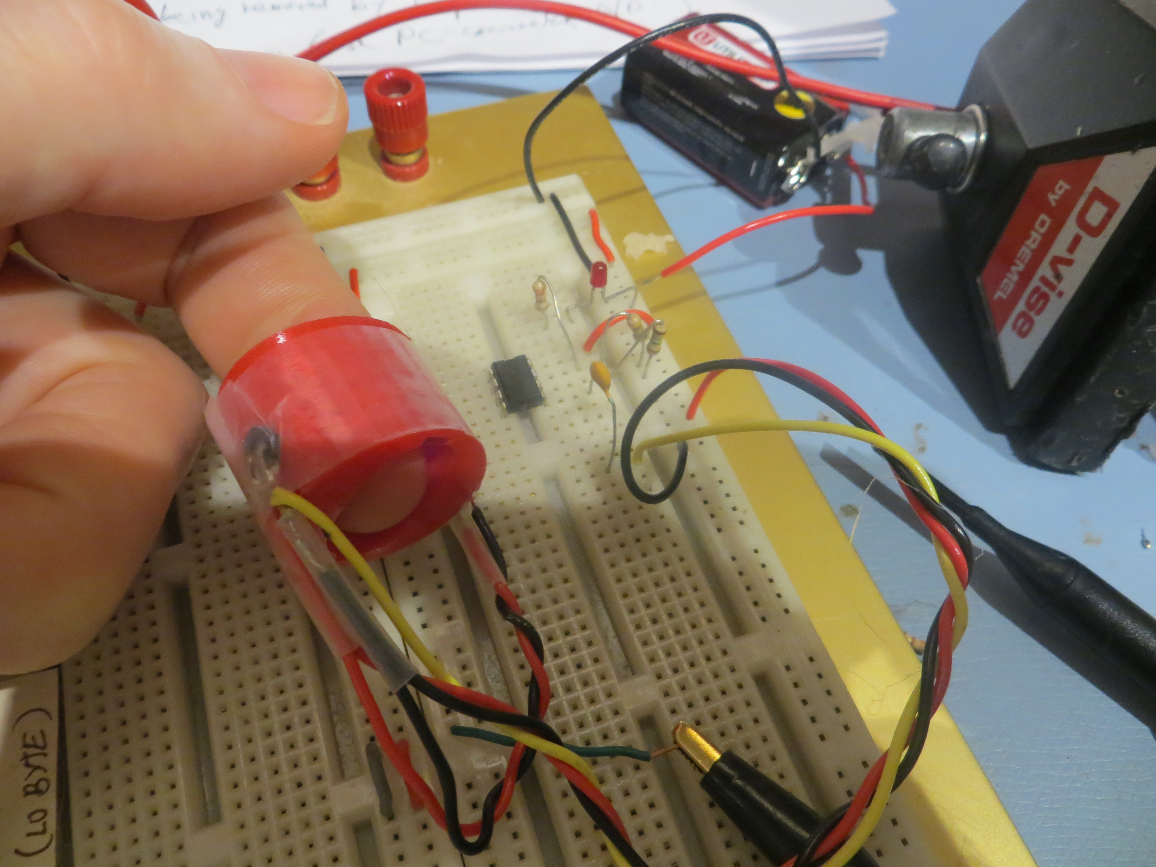
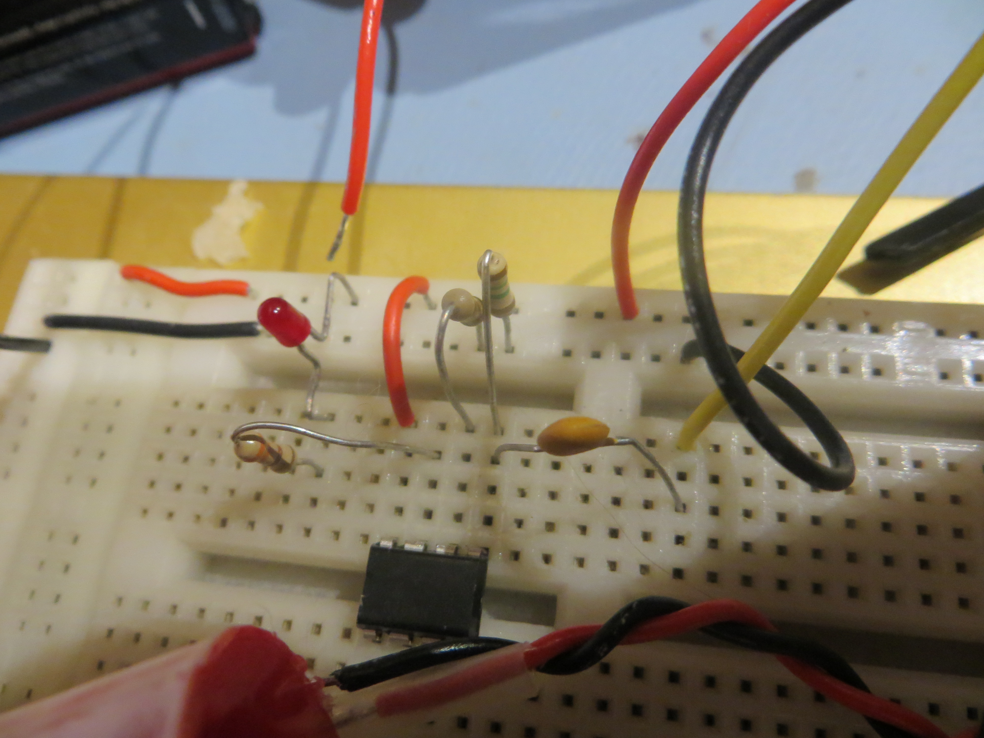
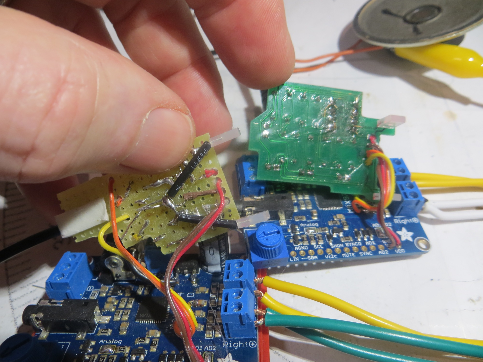
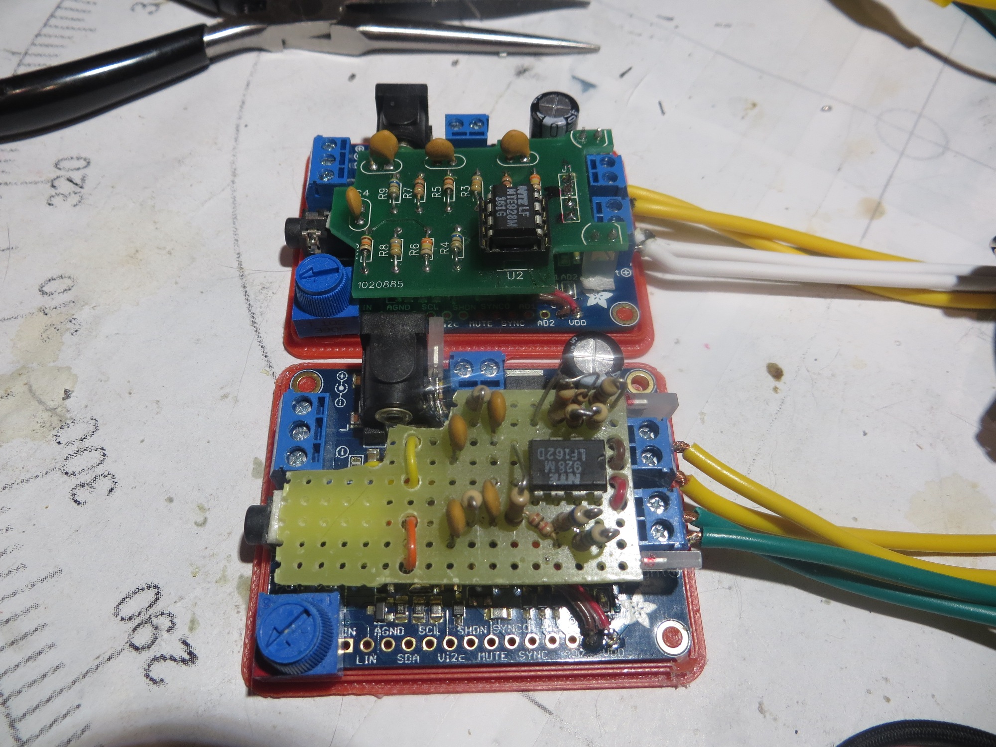
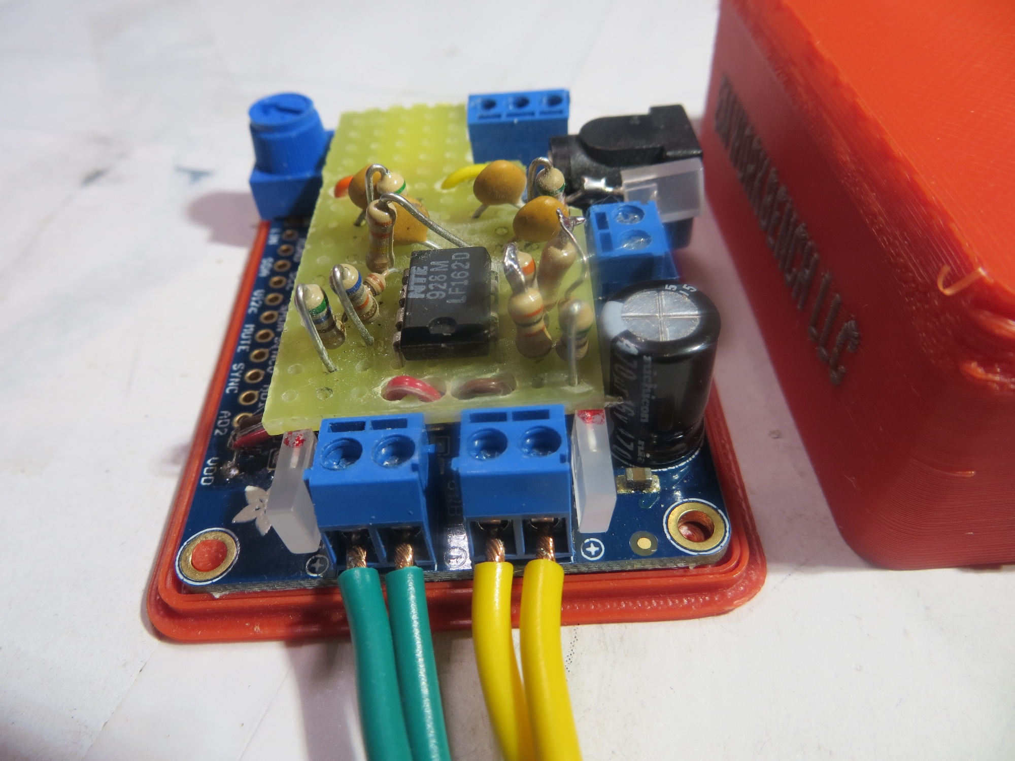
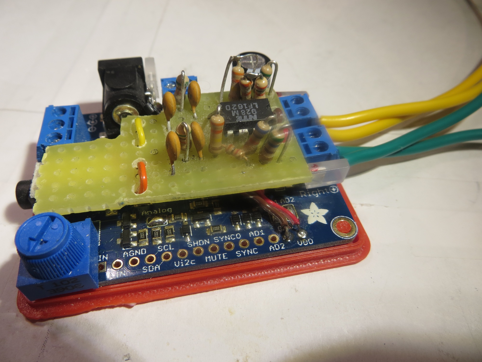
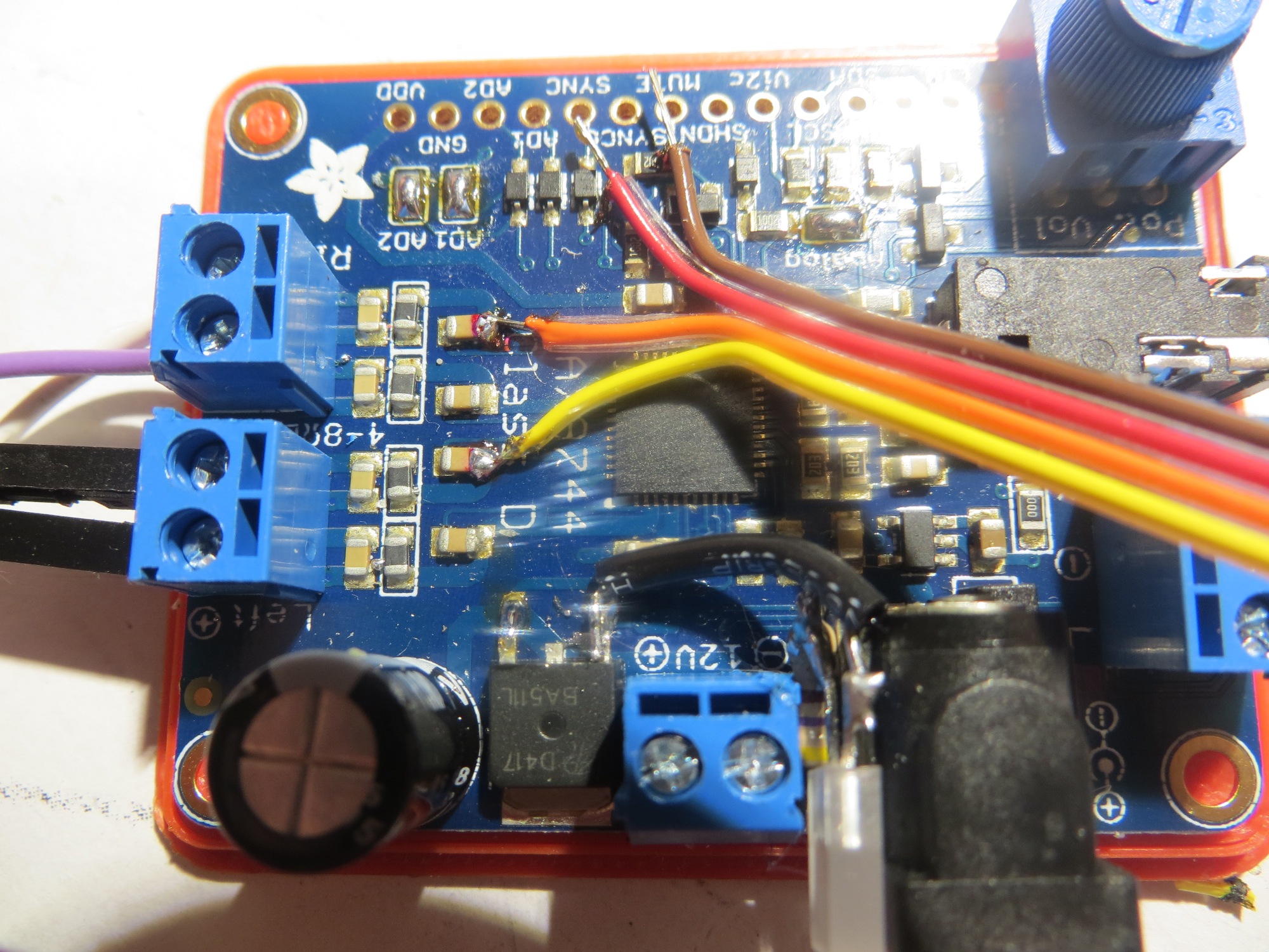
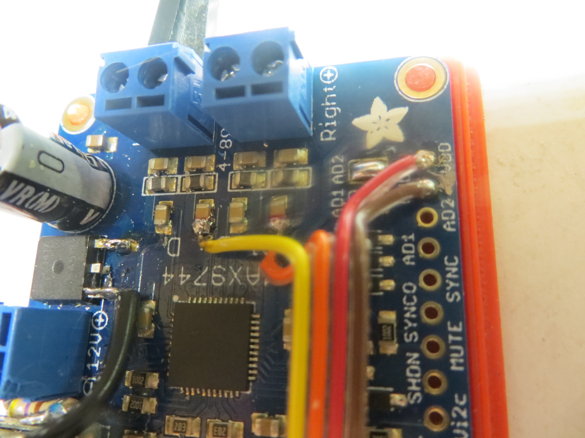
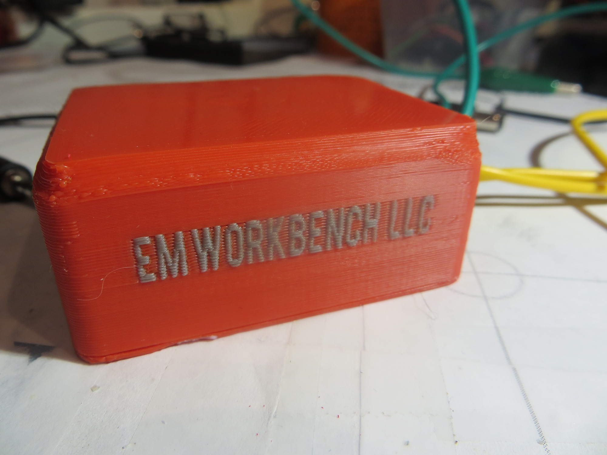
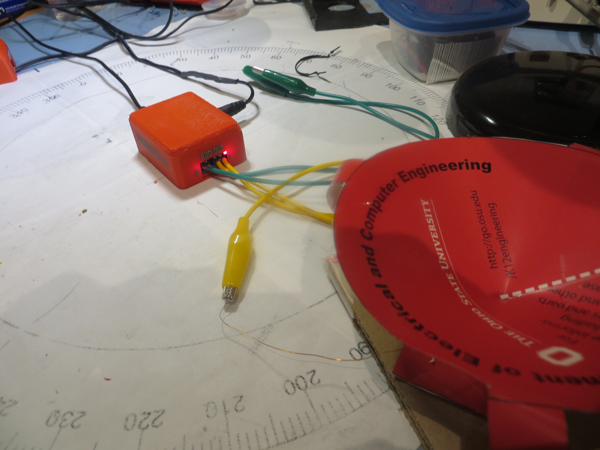
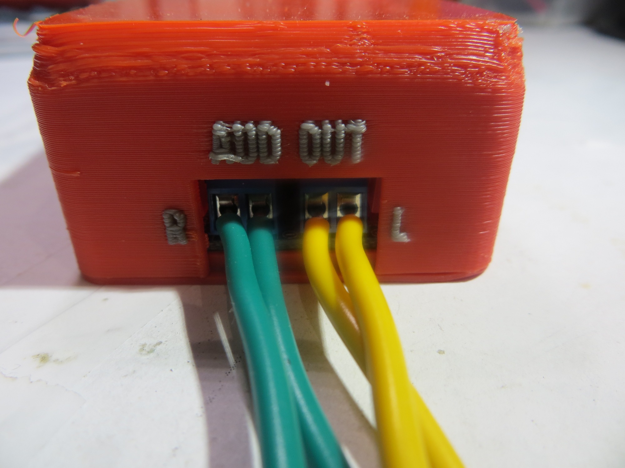
In my last post on this subject, I described the finishing touches on the project to design and fabricate a speaker amplifier for the OSU Engineering Outreach ‘paper speaker’ student project. The ‘finished’ project featured an audio activity monitoring circuit piggybacked onto the Adafruit 20W Class-D amplifier board, using my almost-forgotten hand-wiring techniques on fiberglass ‘perf-board’, as shown in the following images.
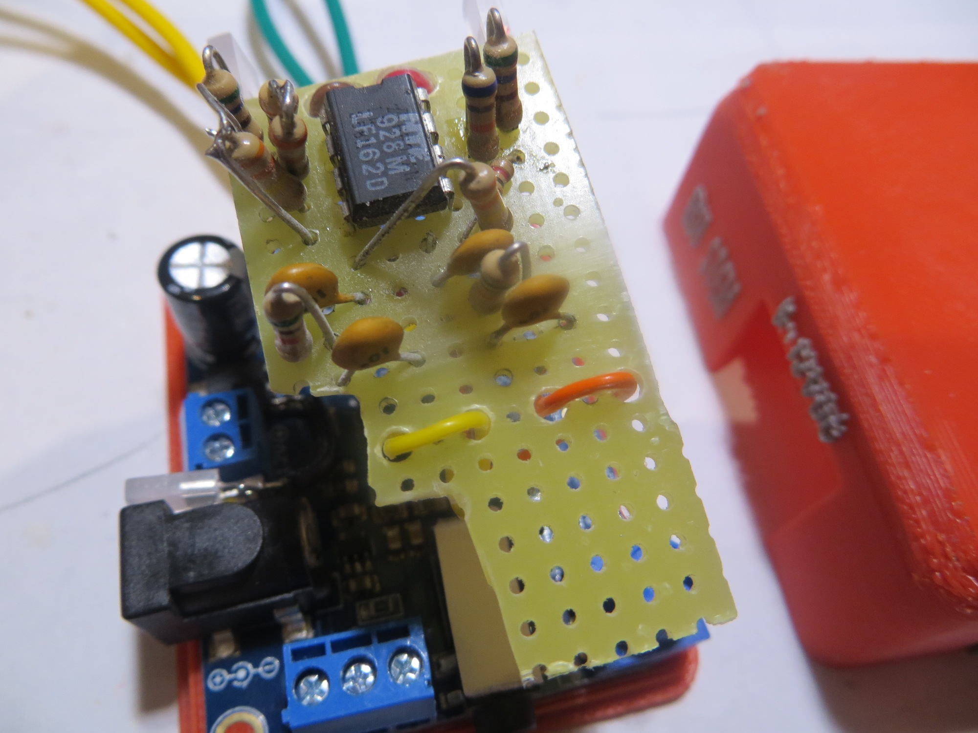
Cut-down perfboard, top view
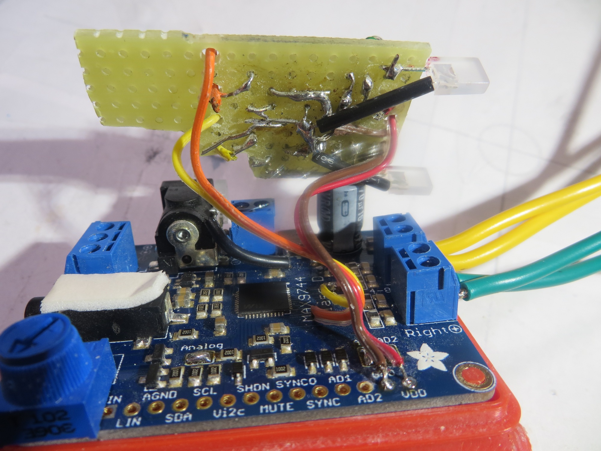
Cut-down perfboard, bottom view
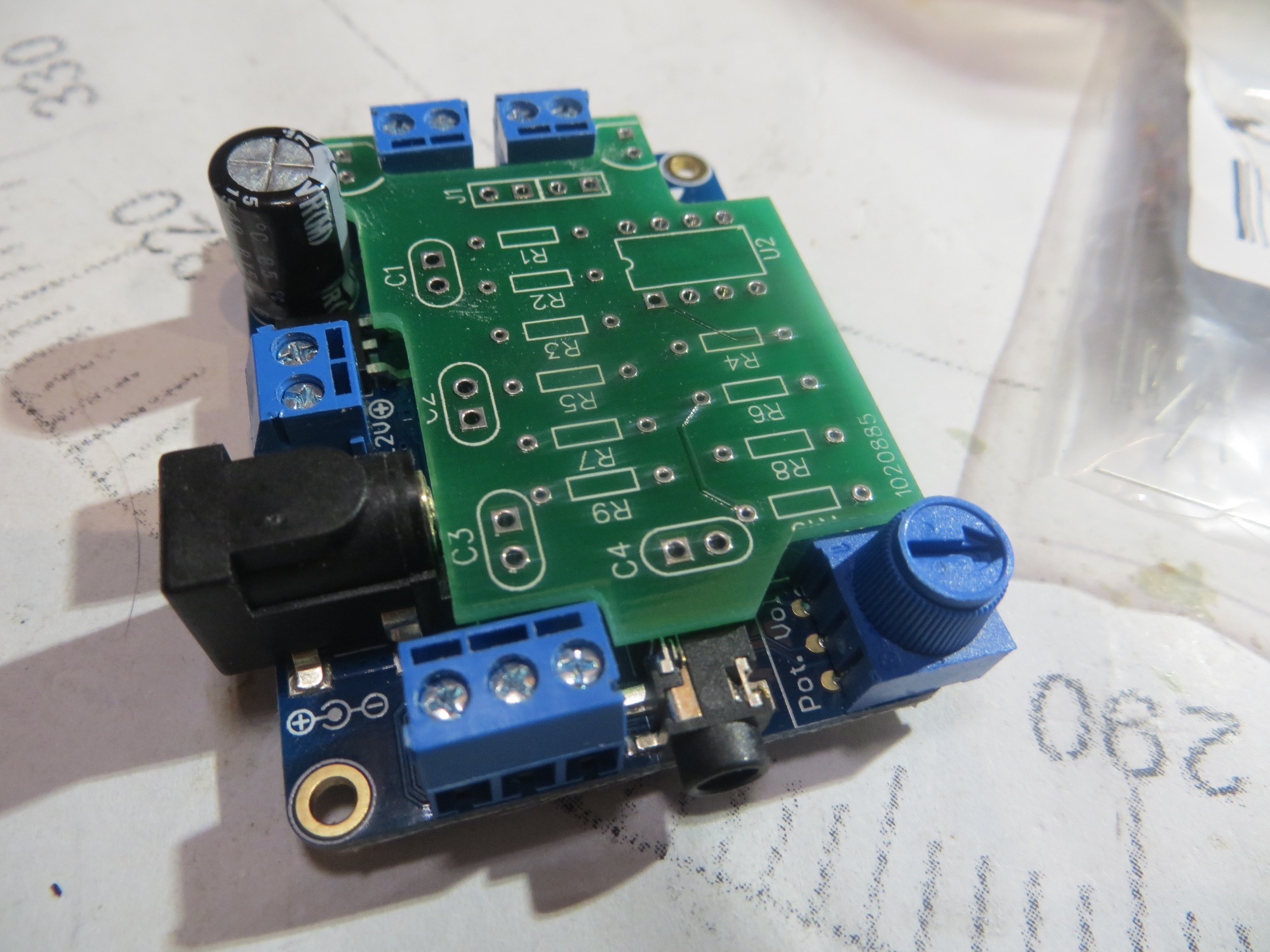
While this technique is perfect for a one-off project, I ultimately wanted to fabricate a number of these amplifier/monitor modules for use by the OSU Engineering Outreach team. So, I decided to investigate the feasibility of obtaining a printed-circuit (PCB) board version of the LED monitor circuit, so I wouldn’t have to hand-fabricate the same circuit multiple times. Of course, I knew in my heart that I could probably hand-fabricate ten (or a hundred) LED monitor circuits in the time it would take me to research the PCB design/fabrication field, acquire and learn a PCB design (aka EDA) package, actually design and implement the PCB, and then have the boards fabricated by a PCB house, but where’s the fun in that?
The last time I dealt with PCB design and manufacture was about 15 years ago while I was a researcher/JOAT (look it up) at The Ohio State University ElectroScience Laboratory, a research lab that specializes in Electromagnetics research and applications. At the time I was a relatively new grad student at the lab (but one with about 30 years of electronics design experience in a prior lifetime with the CIA) and had somehow managed to get involved in a project that required some small-quantity PCBs. The lab’s normal supplier (a local PCB manufacturing house) was still using hand-taping methods and the result was very high priced and of somewhat inconsistent quality (at least in my opinion), so I started looking for ‘a better way’. In short order I found some low-cost, high quality EDA tools, and also found a small PCB house in Canada that would deliver small quantities in about 1/10 the time and 1/10 the cost as the local house. This made me a hero in the eyes of the lab director (but an enemy in the eyes of the guys who were comfortable dealing with the local supplier). Anyway, it’s been another decade or so since I last looked at the EDA/PCB field, so I suspected things were even better now – and I wasn’t disappointed!
After a few hours of Googling, I found a number of posts that indicated that one of the better/easier-to-use EDA packages was Dip Trace, and they had a freeware version for those of us who can get by with 300 pins or less and only 2 signal layers – YAY!! With a little further digging, I found some very complimentary reviews, so I downloaded the ‘free’ version and started trying to refresh my PCB ‘game’. Right away I found that DipTrace has a very complete and readable beginner’s tutorial, and unlike most ‘tutorials’ these days, the DipTrace one doesn’t skip steps – everything is explained and demonstrated in what had to seem like completely unnecessary detail to the experts, but in fact is absolutely crucial for a (almost) first-timer like me. If you are a hobbyist/enthusiast interested in PCB design/fabrication, I highly recommend DipTrace.
After working my way through most of the tutorial, I decided to try my hand at implementing my LED monitor circuit. I started by porting my schematic from Digikey’s ‘scheme-it‘ (a free, browser-based schematic capture utility). Here’s the schematic – first from Scheme-It, and then as it was ported to DipTrace.
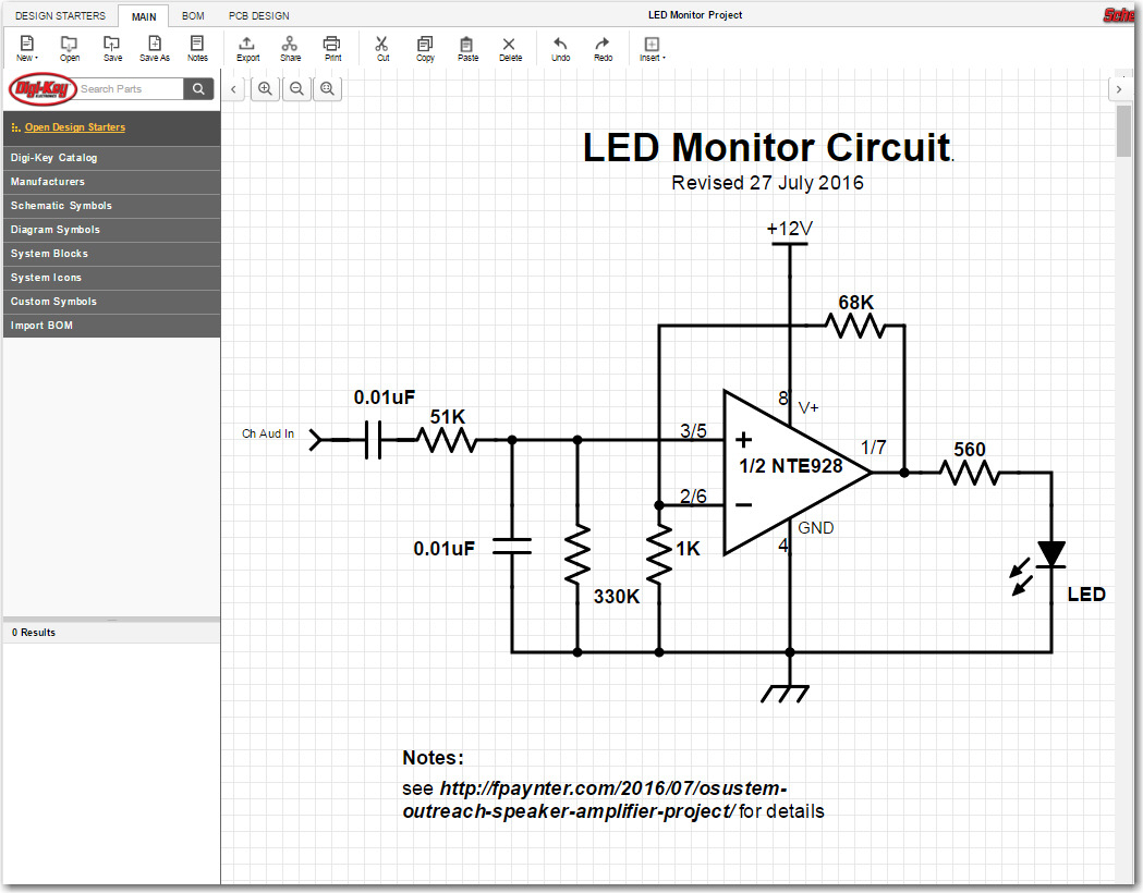
LED Monitor circuit schematic as captured in Digikey’s ‘Scheme-It’ app
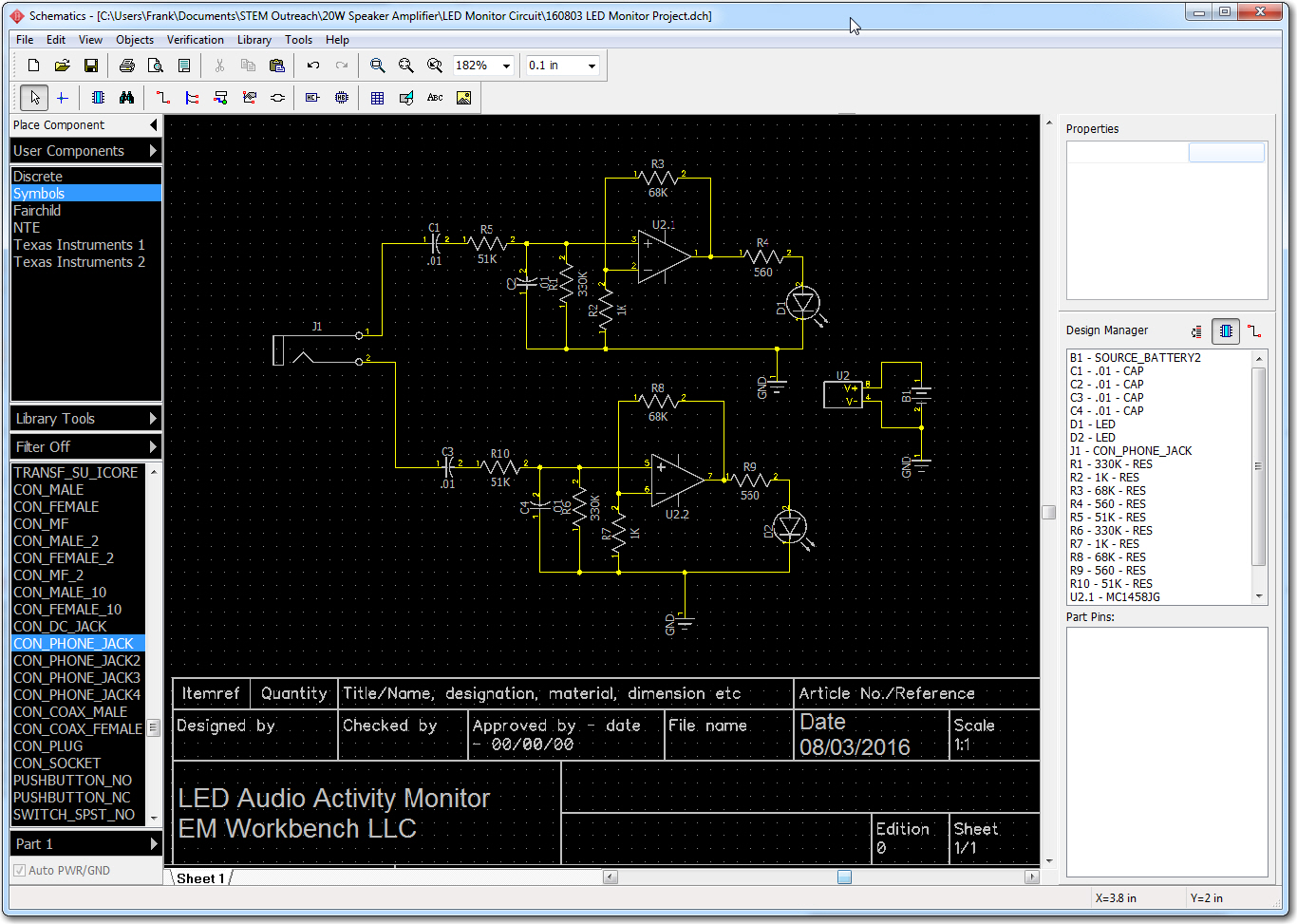
LED Monitor circuit schematic as captured in DipTrace
Following the procedure described (in exhaustive detail – YAY!) in the DipTrace tutorial, I then created an initial PCB design using ‘File -> Convert to PCB’ (or Ctrl-B) in the schematic capture app. This launches the PCB designer, and presents an initially disorganized parts layout as shown below.
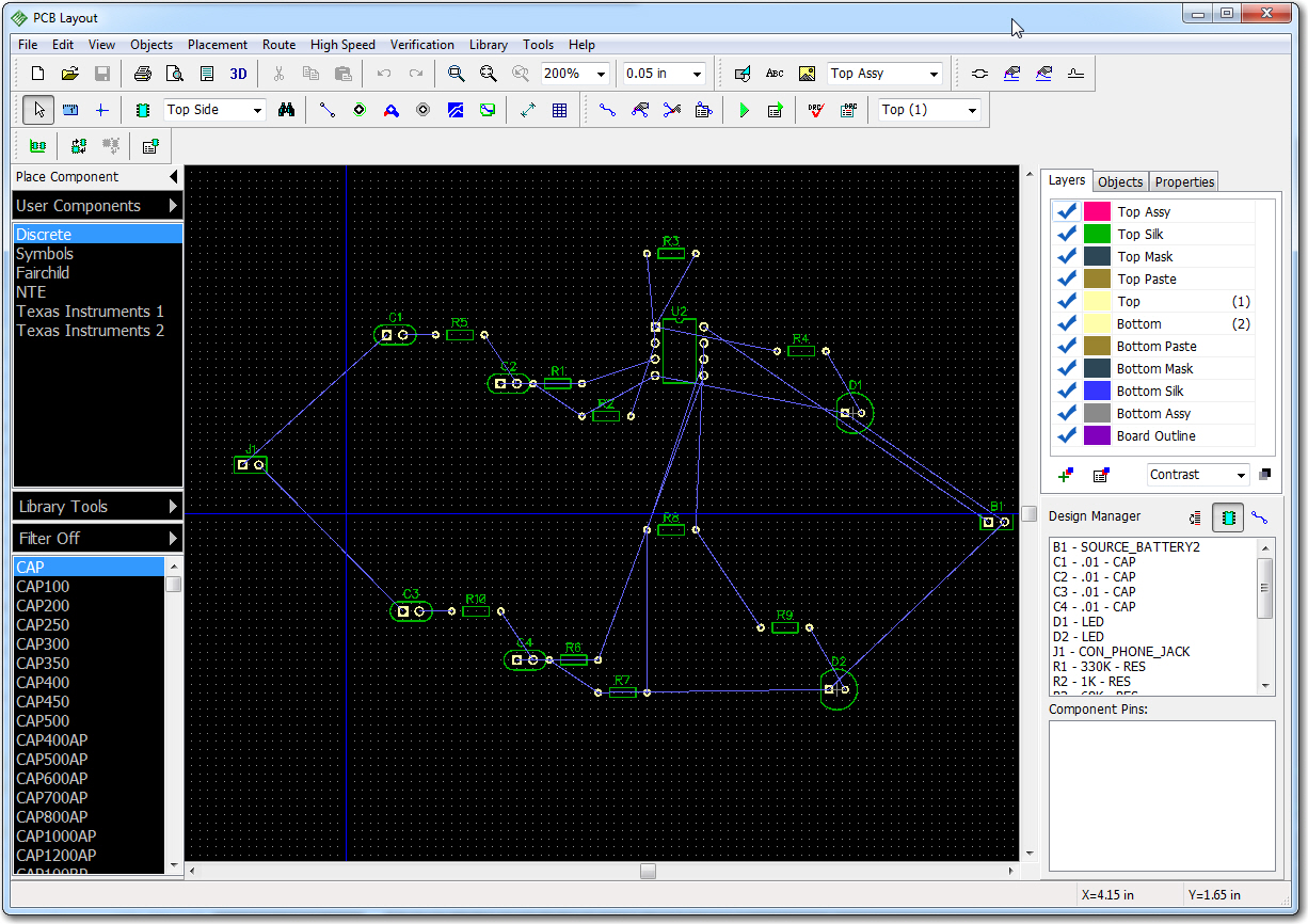
Initial PCB layout
Had it not been for the great tutorial, this mishmash of parts would have been a real turnoff; fortunately, the tutorial had already covered this, so I knew to ‘keep calm and carry on’ by selecting ‘Placement -> Arrange Components’ from the main menu, which resulted in this much more compact and reasonable arrangement.
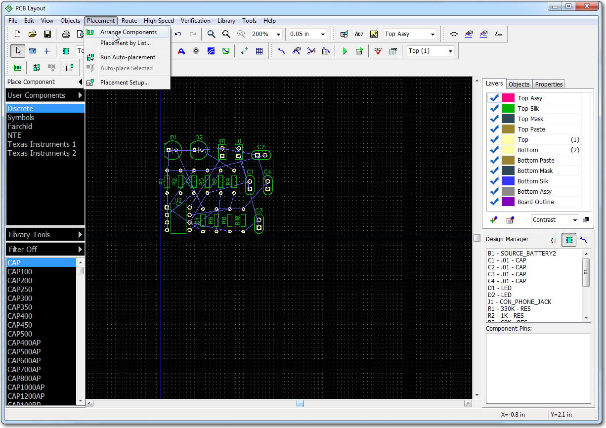
After ‘Placement->Arrange Components’
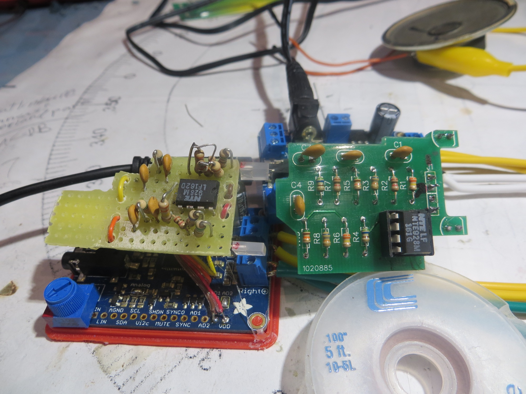
Working back and forth between the tutorial, the actual Adafruit 20W amplifier board, and the PCB design/layout screen, I was able to arrive at a final PCB design that implemented the entire circuit in a form factor that fit into the space available, as shown below.
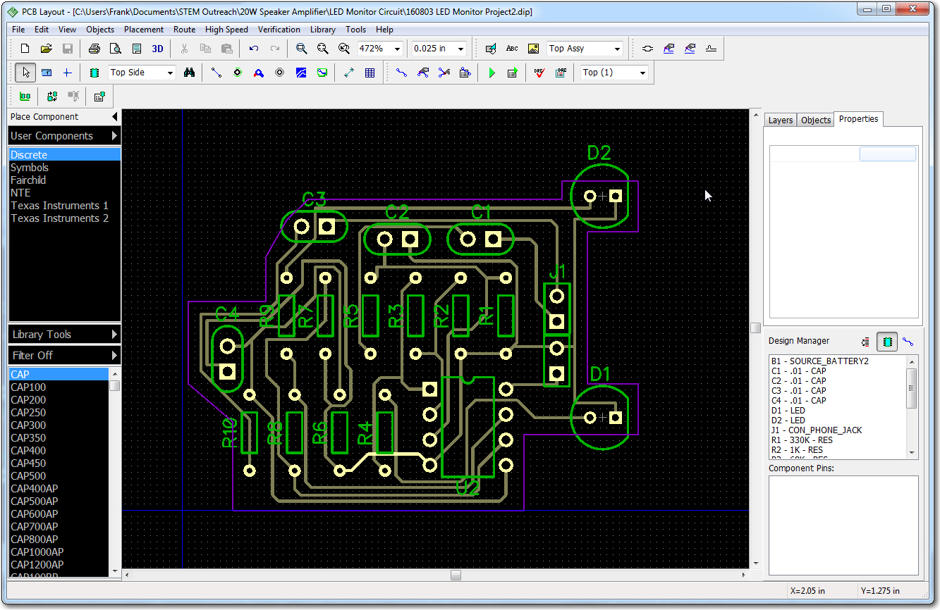
Finished PCB layout. Note the purple board border is customized to fit on top of the Adafruit amp board
The above layout was significantly customized to fit on top of the Adafruit 20W amp board and in the 3D-printed enclosure. This required a number of iterations, but the process was well supported by DipTrace; in particular, the ability to print the layout on my local laser printer in 1:1 scale helped immensely, as I was able to cut it out with scissors and actually lay it on top of the amp board to check the fit.
I was curious about how close I came to the ‘free’ version limitation of 300 pins, so I displayed the ‘File->Layout Properties’ dialog as shown below. From this it was obvious that I still have plenty of room to play with for future projects, although I did use both the available signal layers. ;-).
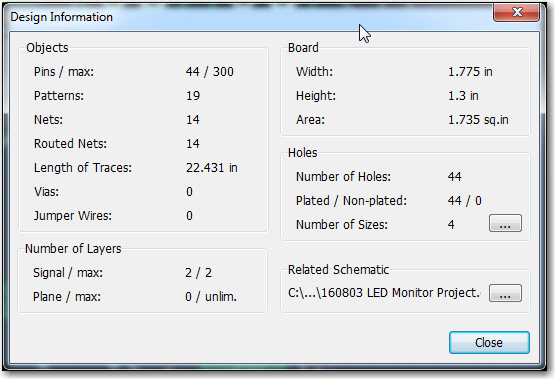
PCB properties, showing that this design fits well within the 300-pin maximum for the ‘free’ version
All in all, I probably spent 2-3 days from start to finish with DipTrace to get a finished PCB layout – not too shabby for an old broke-down engineer who can’t remember where he left his cane and hearing aids ;-).
But, all of this wasn’t even the really cool part of working with DipTrace! The really cool part came when I realized that DipTrace features a ‘baked-in’ link with Bay Area Circuits for PCB procurement (File -> Order PCB…) as shown below
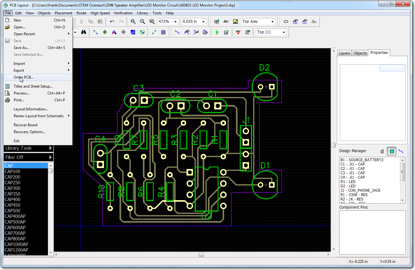
The ‘File->Order PCB’ menu item
When you click on this option, the relevant data is scarfed up from the PCB layout information and you are presented with a simple ordering screen, complete with per-unit and total prices for your design. All you have to do is select the quantity desired and press the ‘Place Order…’ button. No messing with Gerber files, net lists, drilling schedules, mask layouts, etc etc. One button, 30 bucks from my PayPal account – done!!!
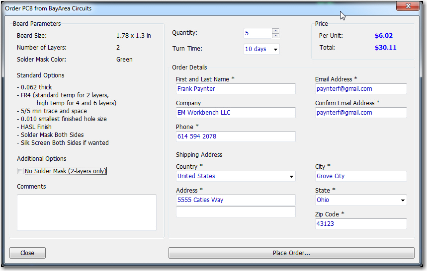
The order detail screen
So, the lead time on the board order was quoted as about 10 days, so I won’t know for a couple of weeks how the whole thing worked out, but I’m quite optimistic. I have to say that this was the most pleasurable and trouble-free PCB design project I have ever experienced, and I have experienced a lot of them over the last 50 years, from hand-cut 10X mylar PCB masks, to hobbyist acid-baths, to $10,000 setup charge custom PCB shops, to this – wow! I may never do another PCB project, but if I do, DipTrace will be my drug of choice!
Stay tuned,
Frank