Author Archives: paynterf

OSU/STEM Outreach Pulse Detector Project


Posted 10/16/2016

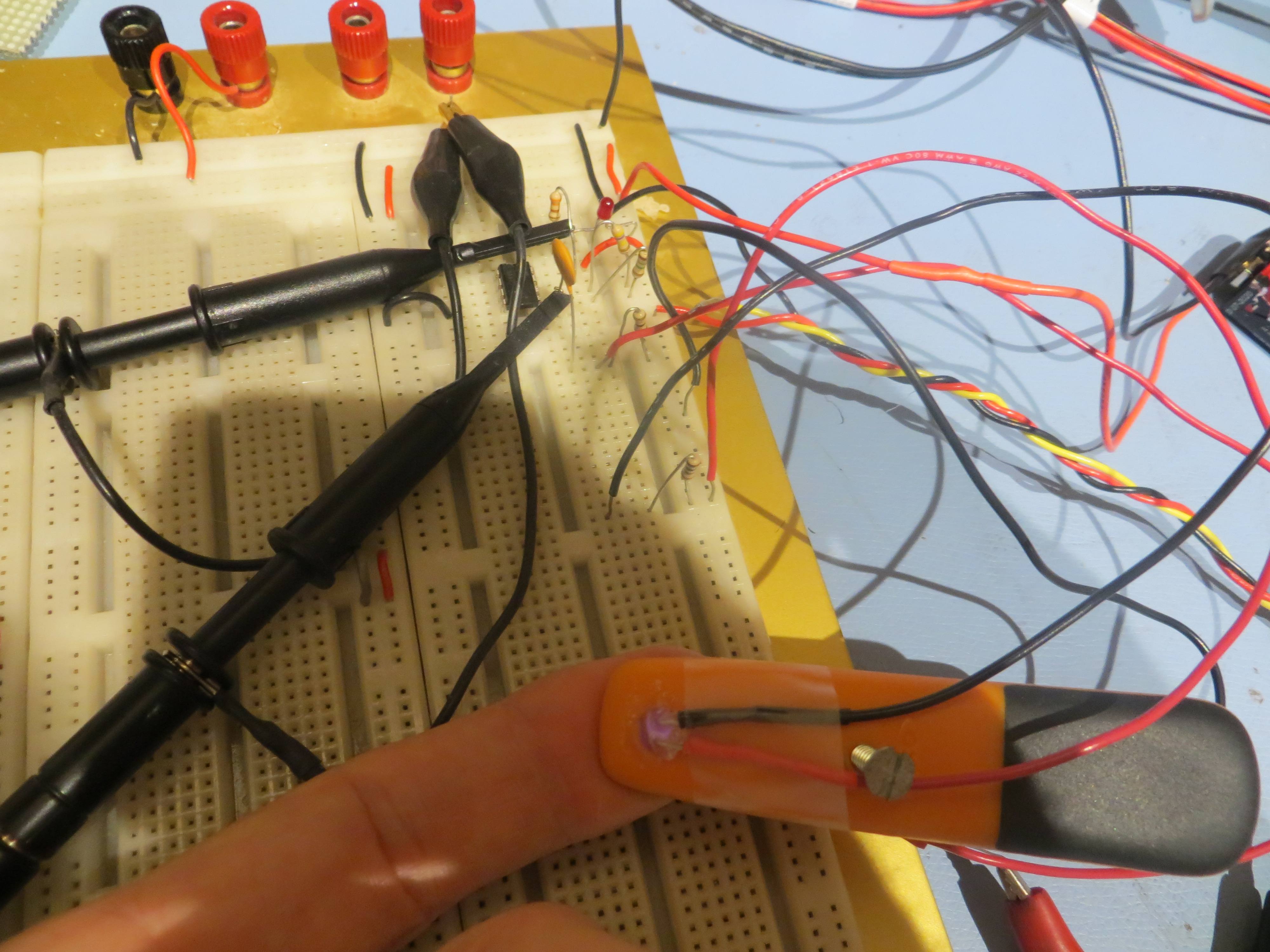
A week or so ago I participated in an OSU STEM Outreach program that showed high-school students how to build a working pulse detector circuit, using a commonly available op-amp and an IR LED/Photodetector pair.  After an initial presentation, the students were given step-by-step instructions for building the circuit on a small plugboard, and I helped when students ran into trouble.  By the end of the one-hour session, most students were successful, and were able to see the output LED illuminate in time with their pulse – cool!

As I helped out with the class, I was a bit shocked to see that the circuit being build by the students required two 9V batteries wired in series to create a +/-9V supply for the op-amp. At the time I just assumed somebody forgot to spec the op-amp to be one with a common-mode range including ground, and the extra battery was the ‘field-expedient fix’ for the problem. When I asked Prof. Betty Lise Anderson about this, she said that a single supply had been tried at one point, but ‘didn’t work out’ for unspecified reasons.   This piqued my interest, so  decided I would investigate the problem a bit further in my home lab.

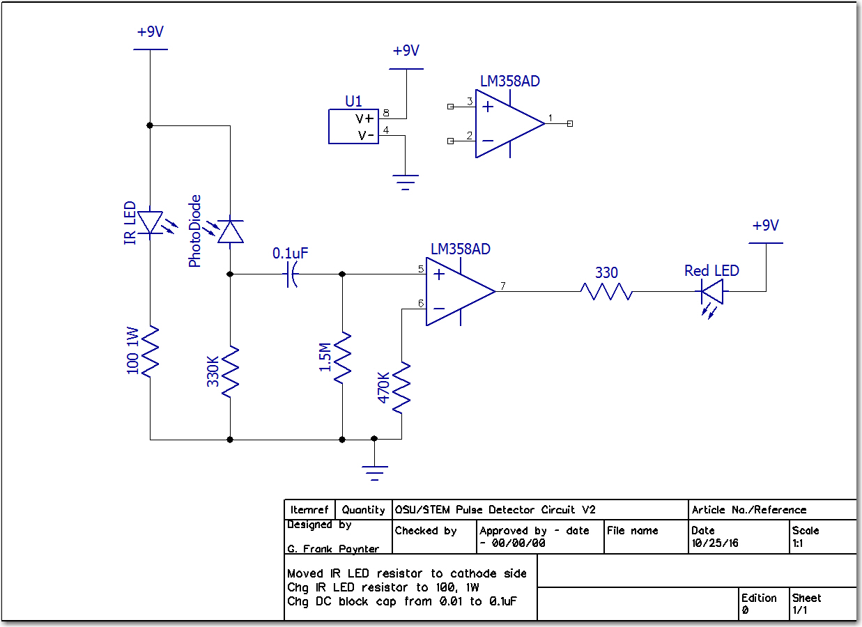
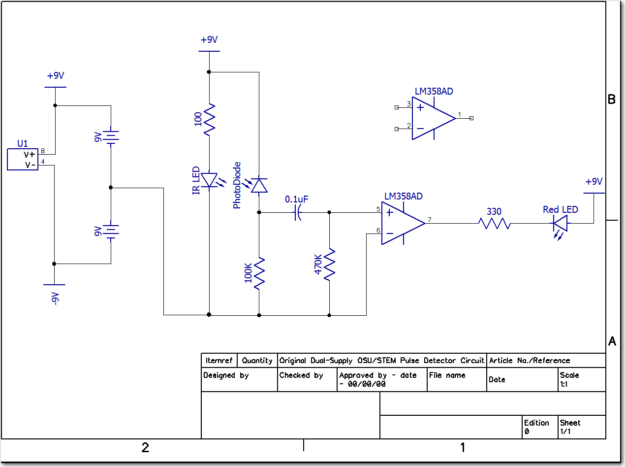
As it turned out, the op-amp being used in the students’ circuits was the ubiquitous dual-LM358  in an 8-pin DIP, and this unit does indeed have a common-mode range including ground, so  the single-supply idea should have worked.  Here’s the original OSU circuit (transcribed into DipTrace’s schematic capture format)

Original OSU Pulse Detector circuit.  Note the dual 9V suppies

Original OSU Pulse Detector circuit. Note the dual 9V suppies

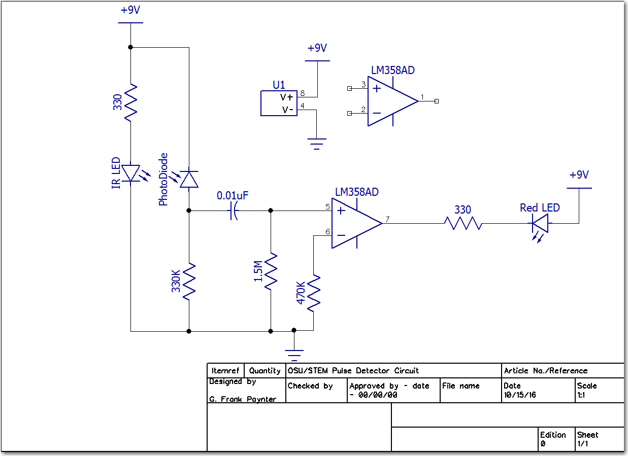
And here’s my final single-supply detector circuit

Final single-supply Pulse Detector schematic

Final single-supply Pulse Detector schematic

Comparing the two, the only real difference is the addition of the 470K resistor from the inverting input to ground.  In the original circuit, the inverting input was tied directly to ground, while the non-inverting input had a 470K to ground.  This can be a problem, as the input bias current for the LM358 can be on the order of 100 X 10-9 (100 pico-Amp), which means that the DC voltage at  the non-inverting input due to bias currents could be as much as 50mV or so.  Since this is on the same order of magnitude as the photo-diode signal at this point, there is a real chance the op-amp would never toggle the output.  The dual-supply setup  eliminates  this problem, but at the cost of a second battery.

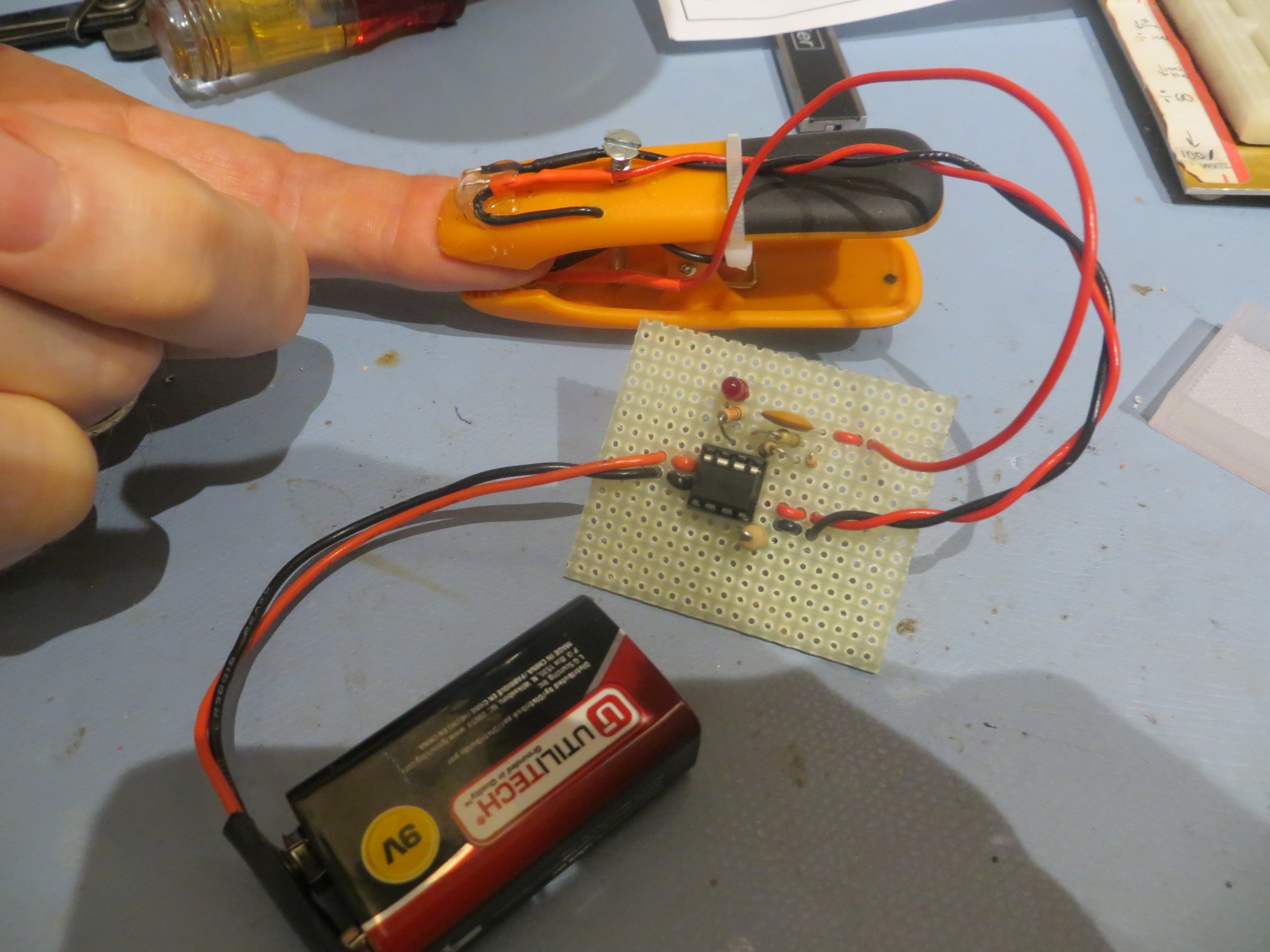
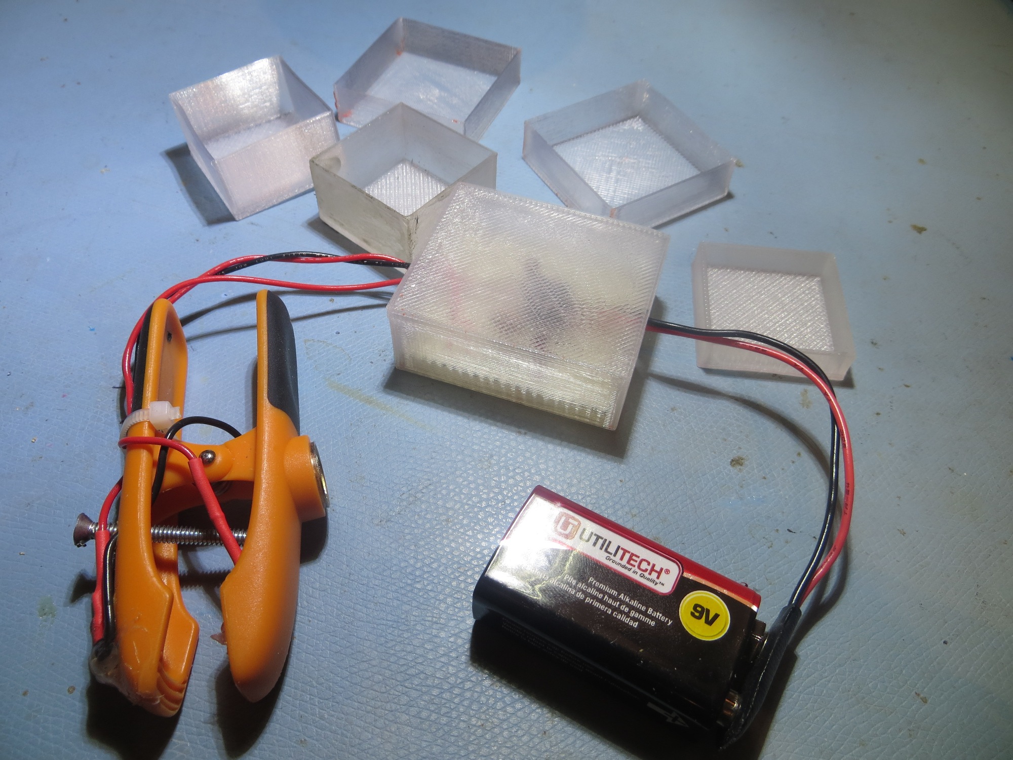
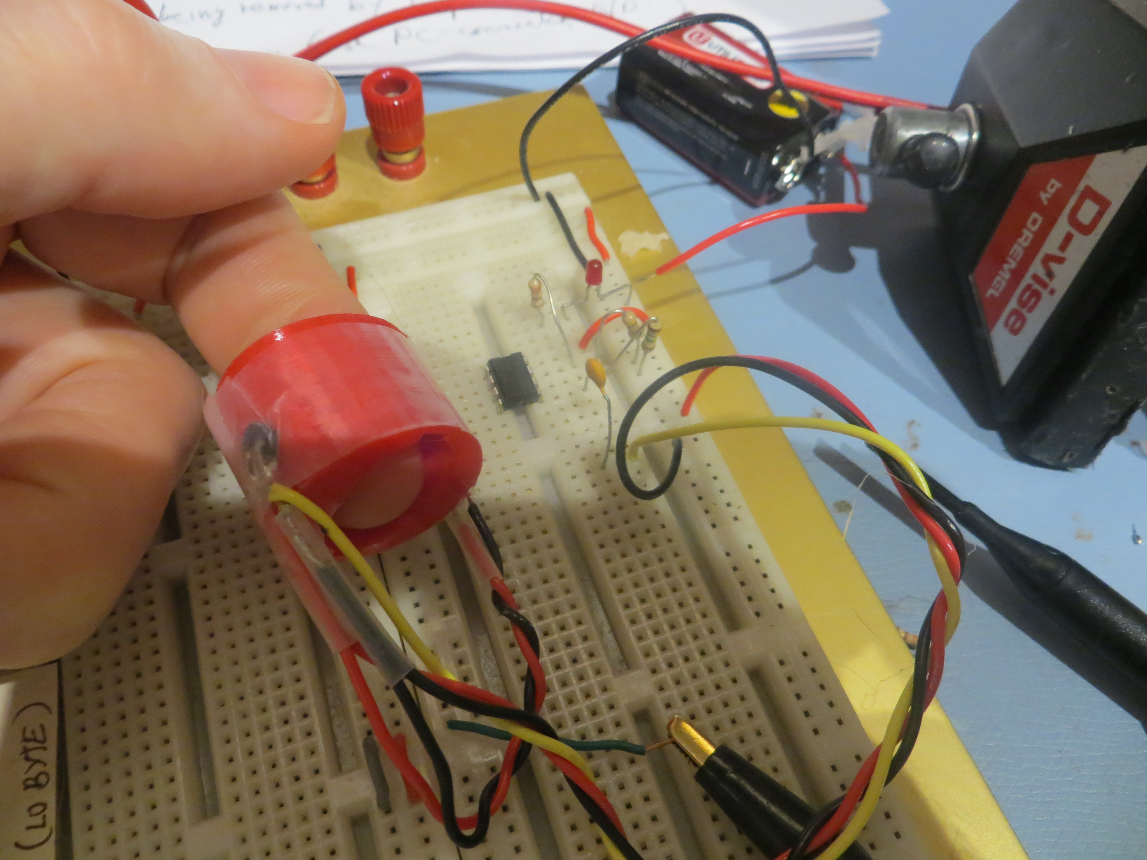
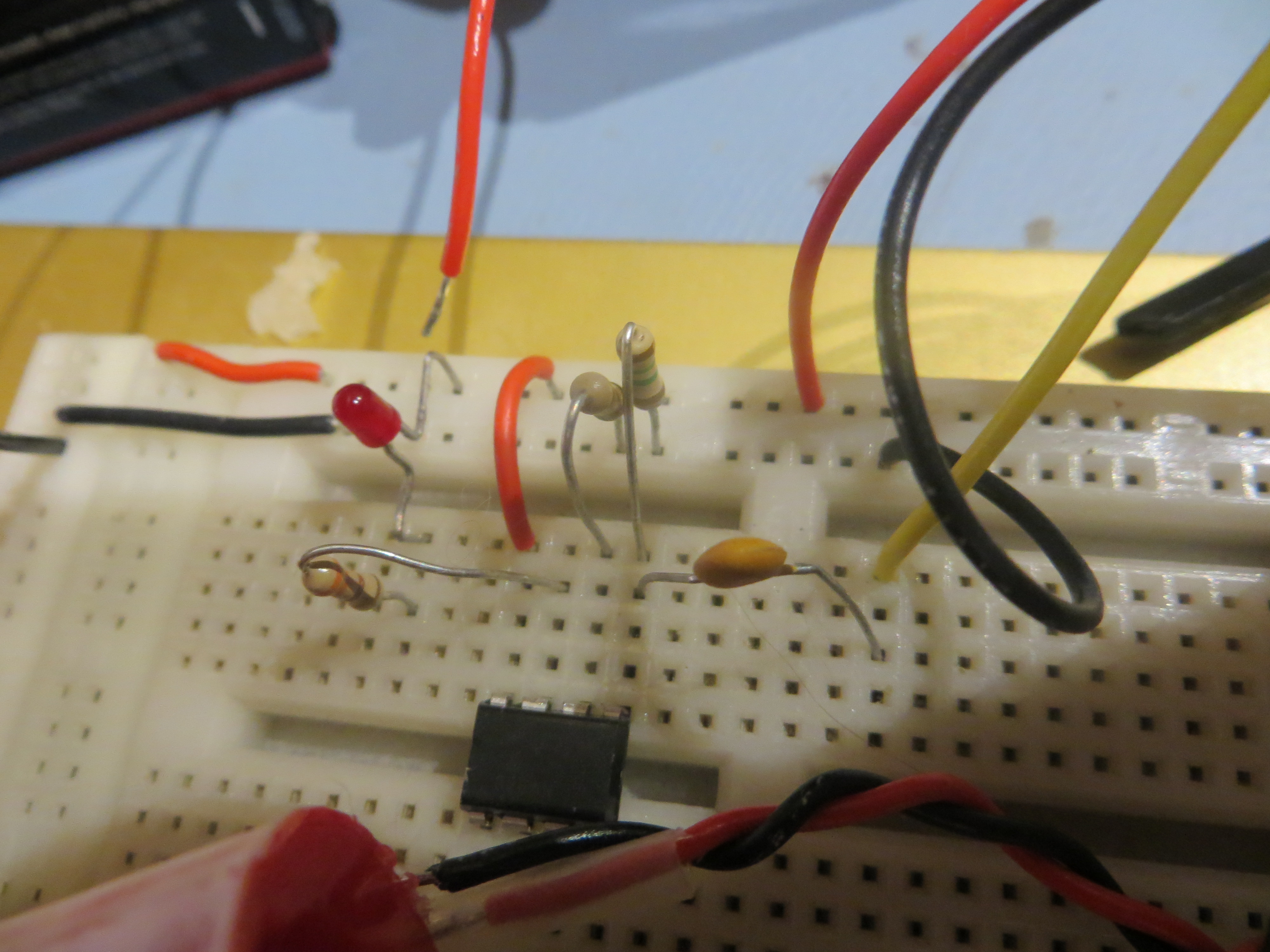
The final circuit, as laid out on my plug-board, is shown below.

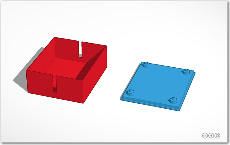
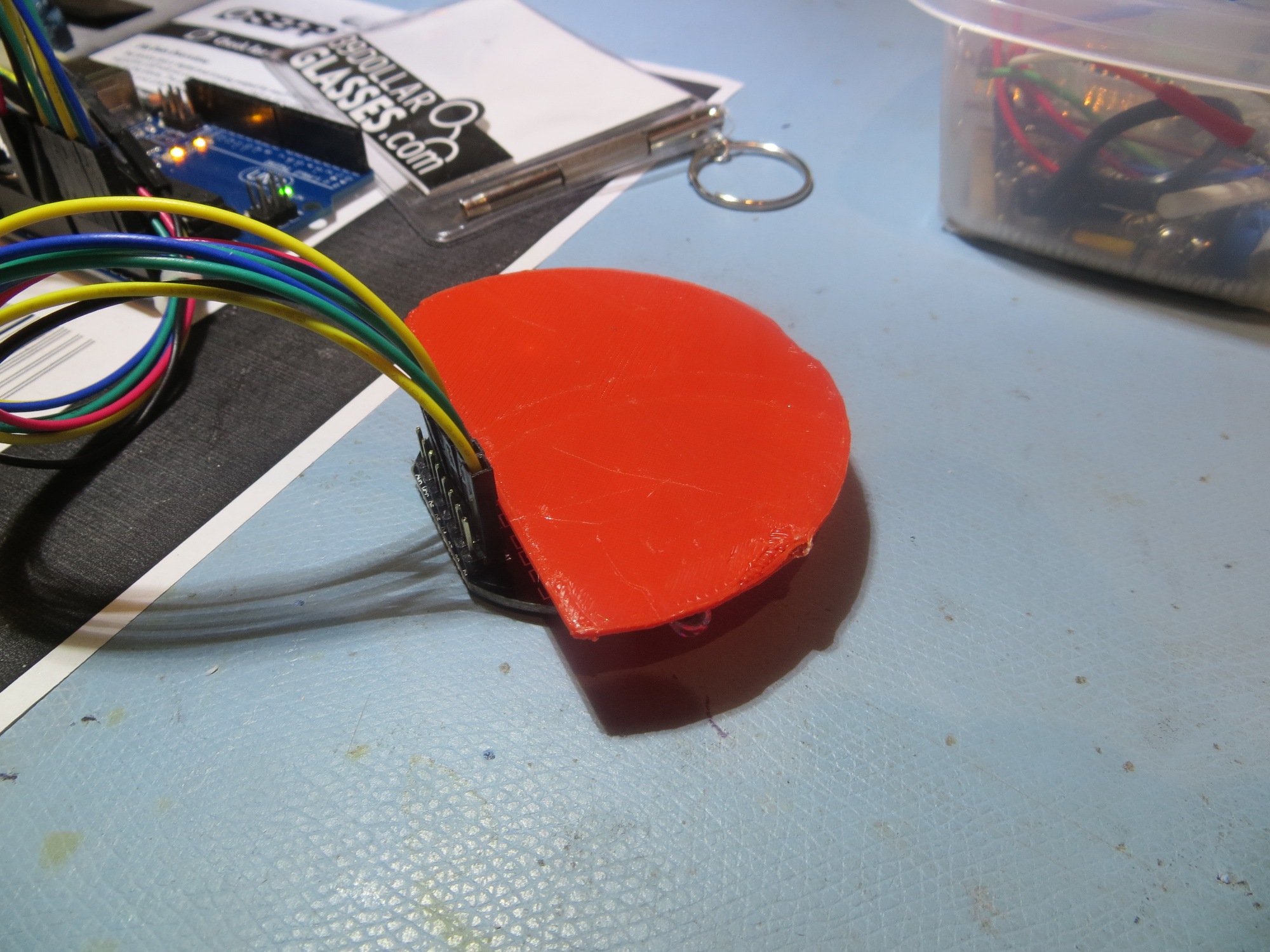
Pulse Detector circuit with my 3D-printed finger socket

Pulse Detector circuit with my 3D-printed finger socket

Final Pulse Detector circuit

Final Pulse Detector circuit

And, because I can, here’s a short movie showing the pulse detector in action ;-).

Wall-E2 Charging Station, Part I

Posted 09/28/16

Ever since I started the Wall-E wall-following project, my goal has been to give Wall-E the ability to periodically recharge his battery without human intervention.  Then Wall-E would be free to roam the house indefinitely, striking fear into the hearts of humans and cats alike! ;-).

The concept for the Wall-E charging station has gone through  a lot of iterations, at least during my drifting-off-to-sleep conceptual design sessions.  Eventually I settled on a concept where Wall-E would be captured by some sort of lead-in railing which would force it onto a raised platform containing the charging power supply.   The platform would contain a set of spring-loaded contacts that would mate with contacts on the underside of Wall-E for charging power and for charging state control.

To start the process, I ran some tests to determine the basic requirements for the lead-in structure.  To support these tests, I modified Wall-E’s code to emulate its tracking behavior, but with an on-off push-button so I could run multiple tests without Wall-E running away.

As the following video snippet shows, my first idea of a low-sided lead-in wall was defeated in short order by Wall-E’s motor torque and soft, knobby wheels.

Speaker Amplifier Project, Part V

Posted 10 September 2016

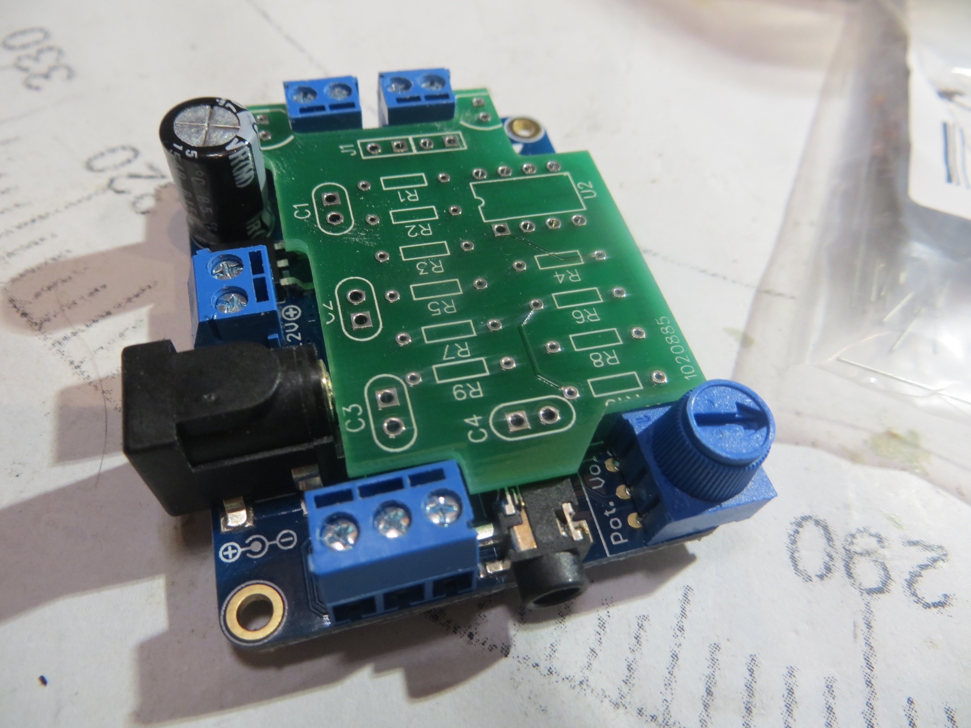
Since my last post on this subject, I have actually gone through two revs of the PCB. The first set was fine electrically (and great quality AFAICT, but I didn’t get the physical border just right, and  I couldn’t file it down enough to fit without breaking a PCB run.  So, I went back to DipTrace, redid the board outline (which also involved some rejiggering of component placement and a bit of manual net editing) and sent off another order to Bay Area Circuits.  After returning from  a week at a duplicate bridge tournament in Atlanta  with my wife, the new rev boards were waiting for me – cool!  The image below shows the new board as installed on the Adafruit 20W amplifier board.

Rev2 PCB installed on Adafruit amplifier

Rev2 PCB installed on Adafruit amplifier

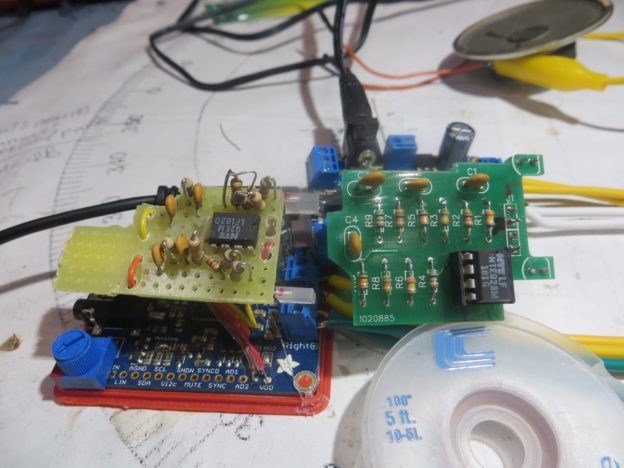
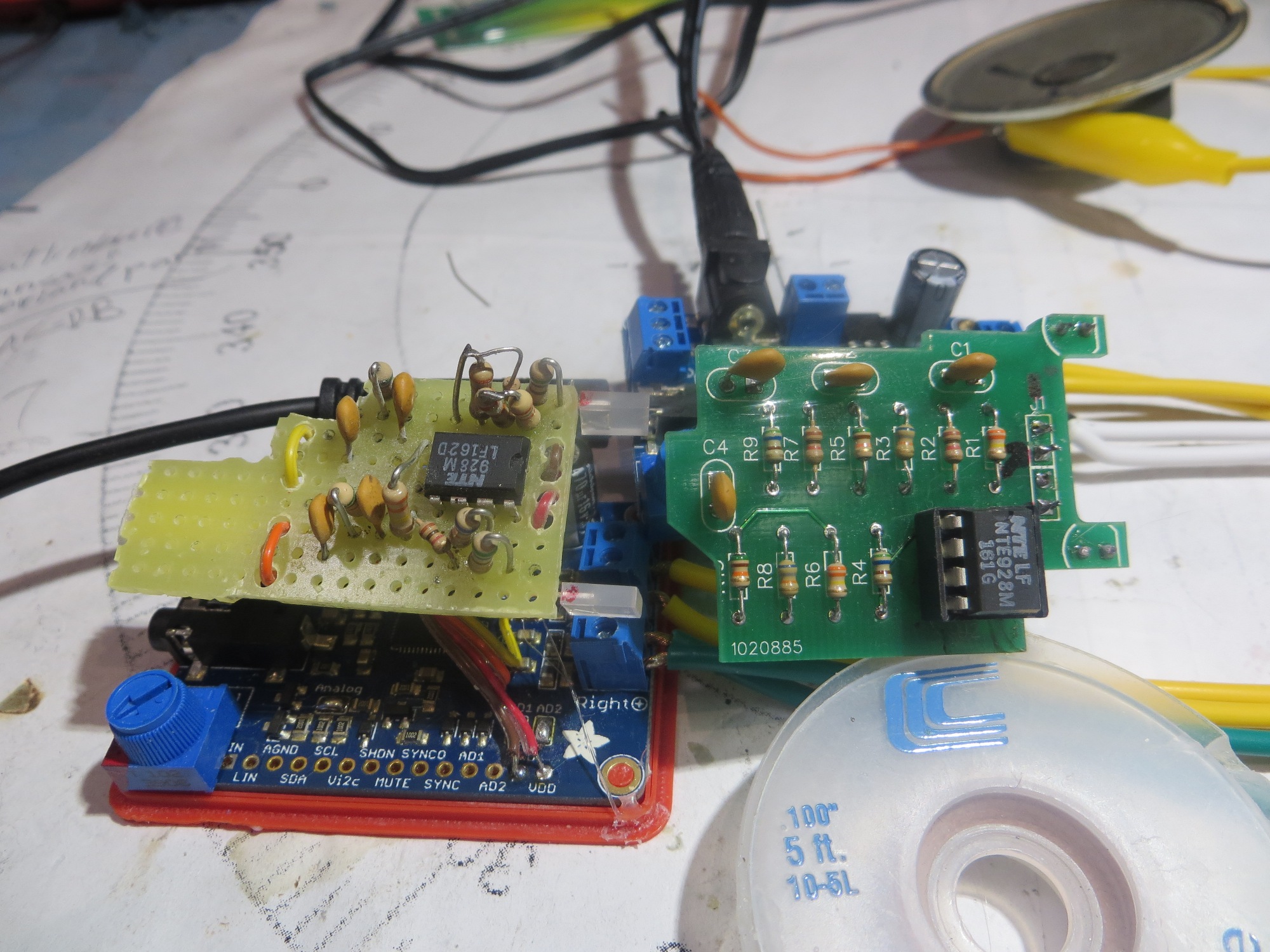
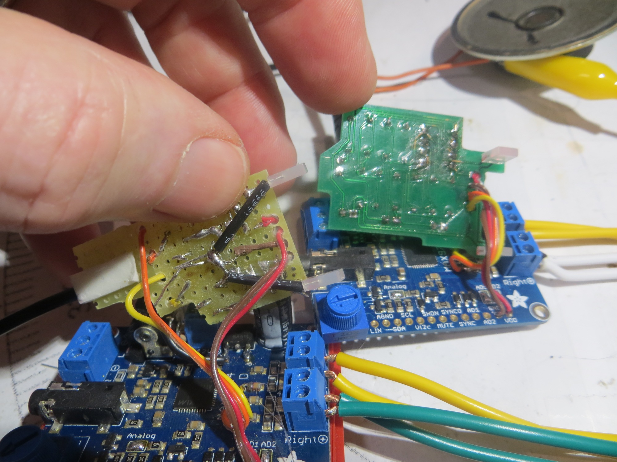
After ensuring that the PCB fit was OK, I populated it, checked all the net connections and resistor values and gave it the old smoke test – and of course it failed – ugh!  I quickly found that the problem was that common-mode range of the the MC748 dual op-amp I was using for the second system doesn’t include ground – oops!  A quick trip to the local Microcenter and the purchase of a wildly overpriced NTE928 dual op-amp solved that problem, but because I was I had soldered the op-amp package directly onto the board (I was  sure this was all going to work, after all), I was now faced with a messy removal and cleanup job.  After getting the old op-amp off and the PCB cleaned up, I installed the new one  (this time, suitably chastised, I installed a socket, and  then installed the op-amp).  The following image shows the finished PCB connected to the amp board, next to the hand-wired original.

Completed PCB connected to Adafruit amplifier

Completed PCB connected to Adafruit amplifier

Bottom of PCB and hand-wired original (note messy area around op-amp)

Bottom of PCB and hand-wired original (note messy area around op-amp)

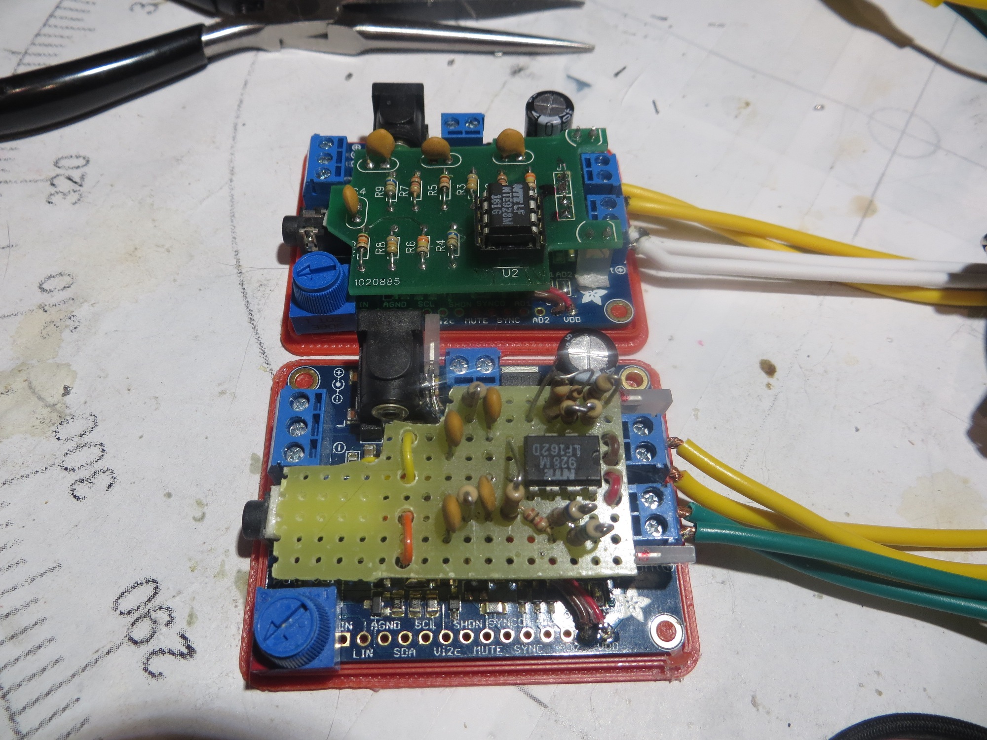
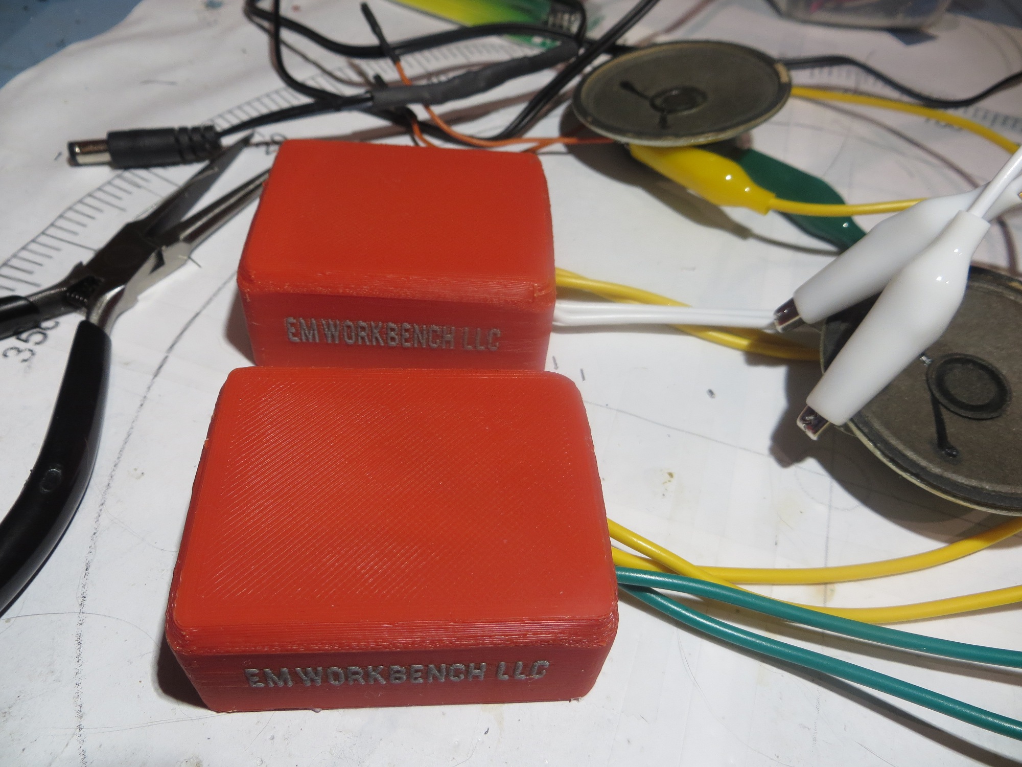
The last thing to do was to get the PCB actually mounted onto the amplifier board, and the assembly into its custom-printed housing, as shown in the following images.

hand-wired and Rev2 PCB mounted to the Adafruit amp boards

hand-wired and Rev2 PCB mounted to the Adafruit amp boards

hand-wired and rev2 PCB mounted in custom-printed enclosures.

hand-wired and rev2 PCB mounted in custom-printed enclosures.

Now all I need is a ‘speaker’ presentation so I can find out if all this work was really worthwhile (actually, I’ve already had a great time with this project, so having it actually work for the students will just be icing on the cake!)


Giving Wall-E2 A Sense of Direction, Part X

Posted 15 August 2016

In my last post on this subject, I described a series of ‘field’ tests of the magnetometer on Wall-E2, my wall-following robot.  These tests demonstrated that the magnetometer was operating properly, but heading results were unusable due to significant distortion of the magnetic field along the west (garage-side) wall of the entry hallway.

This post describes a similar test in an interior hallway. The interior hallway in our home is oriented orthogonally to the entry hallway, i.e. at 110/290 deg magnetic. The walls are about 1 m wide, and constructed of standard wooden stud and sheet rock construction.  There are several rooms opening off this hallway, but all the entry doors were closed for this test.

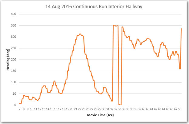
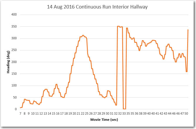
As shown in the movie and the associated Excel chart, the robot starts at the west end headed east, travels the length of the hallway, maneuvers around for a while, and finishes up headed west.  During the first and last 10-15 seconds of the run, Wall-E2 is physically heading in a more or less constant direction (about 110 deg in the first part, about 290 deg in the last part).

Wall-E2 heading results from interior hallway run

Wall-E2 heading results from interior hallway run

Unfortunately, the Excel chart shows a different story.  During the first 15 seconds of the run, there is a definite linear change in the average heading, from about 25 deg to about 75 deg, even though the robot is physically tracking along a wall that is oriented at about 110/290 deg.  During the last 15 seconds or so, the opposite happens; there is a linear downward trend from about 300 deg to about 225 deg.   These trends are physically impossible, so the only possible explanation is that either the magnetometer readings are in error, or there is something in or near the interior hallway that is distorting the earth’s magnetic field enough to produce these results.

I had hoped that the interference noted in the previous post was due to the common wall with the garage and its associated metal structures,  and that the interior hallway would be free of such problems, but apparently this is not the case.  So, I’m now forced to consider other ideas for interior geo-location.

Stay tuned!

Frank

Giving Wall-E2 A Sense of Direction, Part IX

Posted 12 August 2016

For the last several months (or was it years – hard to tell anymore) I have been trying to implement a magnetic heading sensor for Wall-E2, my wall-following robot.  What started out last March as “an easy mod” has now turned into a Sisyphean ordeal – every time I think I have one problem figured out, another (bigger) one pops up to ruin my day.  The first problem was to  re-familiarize myself with the CK Devices ‘Mongoose’ IMU, and get it installed on the robot.  The next one was to figure out why it didn’t work quite the way I thought it should, only to discover that sensitive magnetometers don’t really appreciate being installed millimeters away from dc motor magnets – oops!  So, that little problem led me into the world of in-situ magnetometer calibration, which resulted in my creation of a complete 3D magnetometer calibration utility  based on a MATLAB routine (the tool uses Windows WPF for 3D visualization, and Octave for the MATLAB calculations – see this post).  After getting the calibration tool squared away, I used it to calibrate the Mongoose unit (now relocated to Wall-E2’s top deck, well away from the motors), and once again I thought I was home free.  Unfortunately, reality intruded again when my ‘field testing’ (in the entry hallway of my home) revealed that there were places in the hallway where the  magnetometer-based magnetic heading reports were wildly different than the actual physical robot orientation, as reported in my July post on this subject.

After the July tests, I knew something was badly wrong, but I didn’t have a clue what it was, so I decided to put the problem down for a while and let my subconscious poke at it for a while.  In the interim I had a wonderful time with my two grandchildren (ages 13 & 15)  and a real 3D printing geek-fest with the younger of the two.  I also got involved in creating a small audio amplifier in support of the Engineering Outreach program here at ‘The’ Ohio State University.

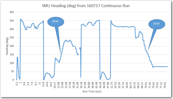
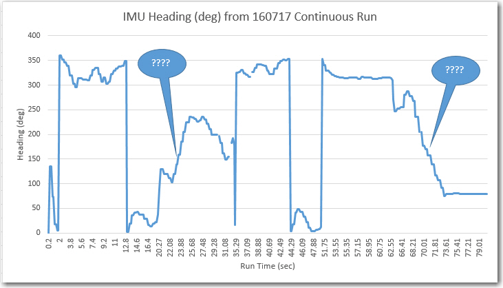
So now, after almost a month off, I’m back on the case again, trying to make sense of that clearly erroneous (or at least non-understandable) data, as shown below (repeated from my previous post)

July continuous run test, showing two areas where the reported headings don't match reality

July continuous run test, showing two areas where the reported headings don’t match reality

The two areas marked with ‘???’ correspond to the times where the robot was traversing along the west (garage side) wall of the entry hall, the first time going north, and the second time going south.  The robot was clearly going in a mostly constant direction, so the data obviously doesn’t reflect the robot’s actual heading.  However, on the other (east) side of the entry hallway, the data looks much better, so I began to think there was maybe something about the west wall that was screwing up the magnetometer data.

As usual with experimentation, it is important to design experiments where the number of variables is kept to the minimum, ideally just one.   By keeping all other parameters fixed, any variation in the data must be due solely to that one variable.  In this case, there were several variables that needed to be considered:

  • The anomalous data might be due to some changes in motor current.    When the robot is wall following, there are constant small changes  to the left & right motor currents.  When the robot encounters an obstacle, it backs up and spins around, and this entails radical changes in motor current direction and amplitude.
  • The anomaly might be due to some timing issue.  It could be, for instance, that the heading  data from the  magnetometer is coming in too fast for the comm link to handle, so it starts becoming decoupled from the actual robot position/orientation, and then catches up again at some other point.
  • The anomaly might be due to some physical characteristic of the entry hallway.  The west side is where the most obvious anomalies occurred, and that wall is common with the garage.  Maybe something in the garage (cars, tools, electrical wiring, …) is causing the problem.

Using my new magnetometer calibration utility, Wall-E2’s magnetometer has been  calibrated with the motors running and with them off, and there was very little difference between the two calibration matrices.  Moreover, my bench testing has shown very little heading change regardless of motor current/direction.  So although I couldn’t rule it out completely, I didn’t see the first item above as a  viable suspect.

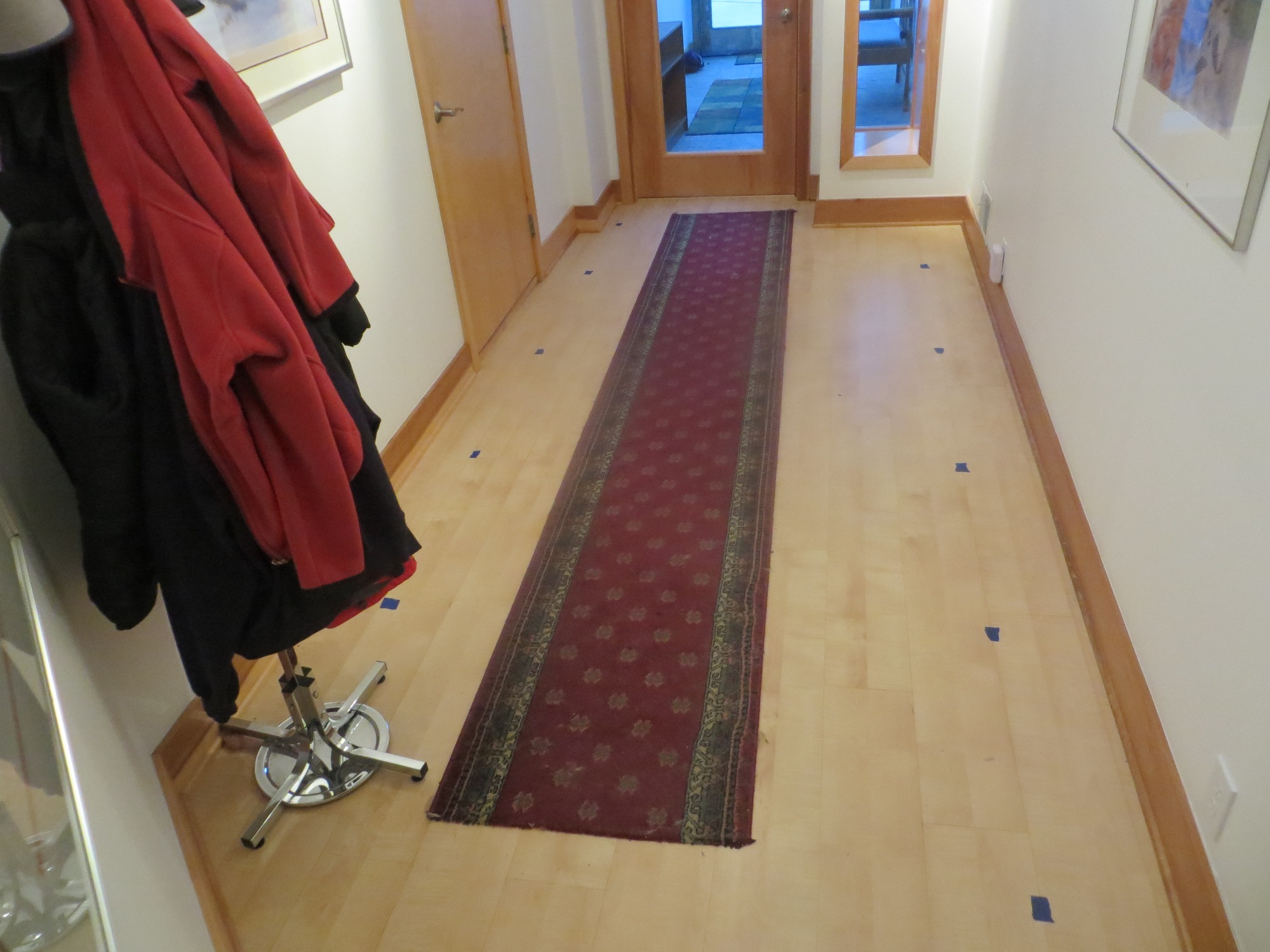
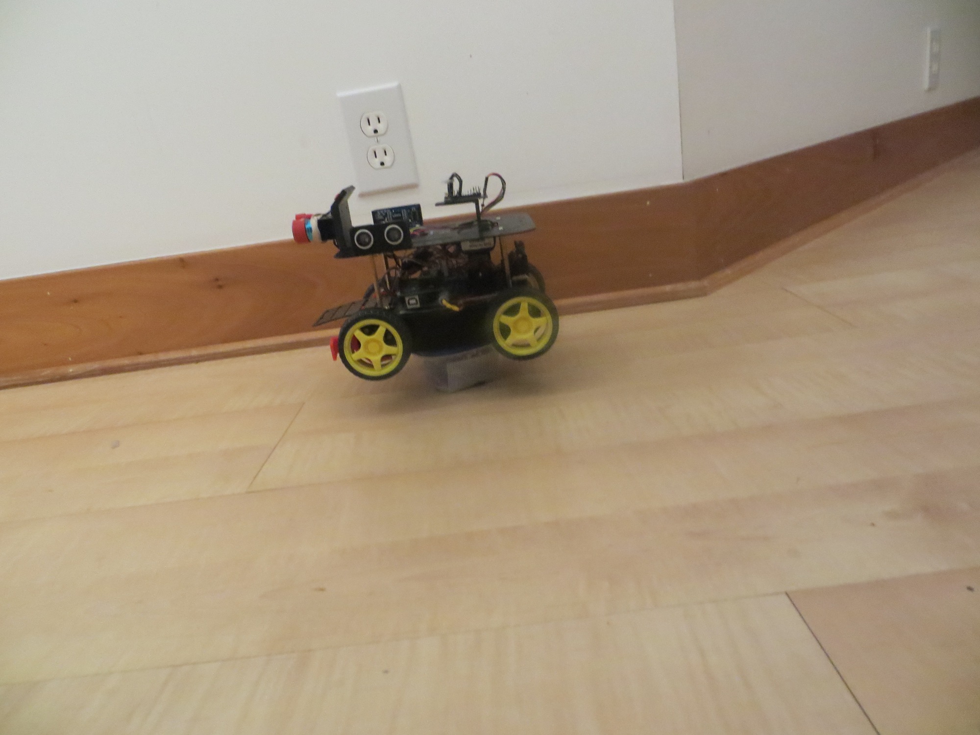
Although I haven’t seen any timing issues during my bench testing, this one remained a viable suspect IMHO, as did the idea of a physical anomaly, so my experimental design was going to have to discriminate between these two variables.  To eliminate timing as the root cause, I ran a series of experiments in the entry hallway where the robot was placed on a pedestal (so its wheels were clear of the floor) at several fixed spots in the entry hallway, and heading data was collected for several seconds at each point.  The following images show the layout and the robot/pedestal arrangement

Experimental layout. Blue spots correspond to numbered/lettered position in layout diagram

Experimental layout. Blue spots correspond to numbered/lettered position in layout diagram

Wall-E2 on a pedestal so motors can run normally without moving the robot

Wall-E2 on a pedestal (at position ‘A’ in diagram) so motors can run normally without moving the robot

10-12 August Mag Heading Field Test Layout

10-12 August Mag Heading Field Test Layout

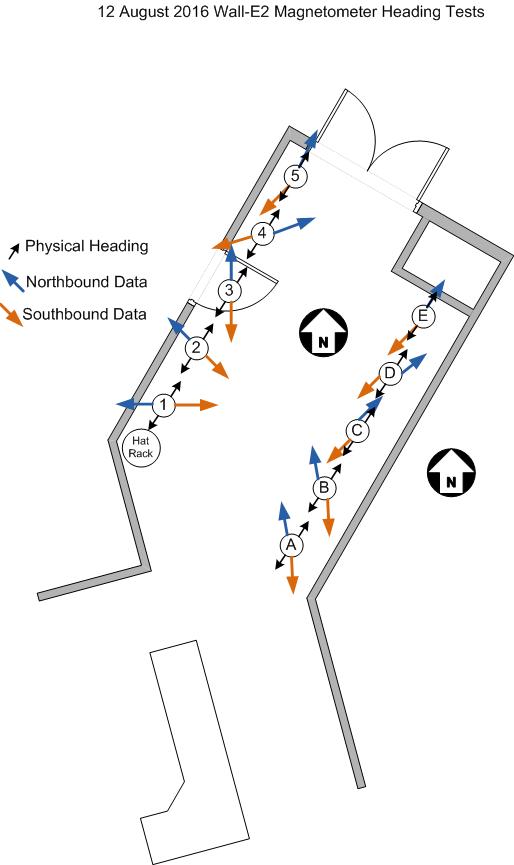
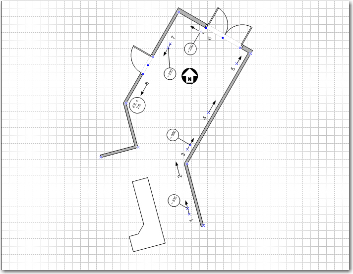
Data was collected at the positions shown by the  numbers from 1 to 5 along the west (garage) wall, and by the letters from A to F along the east wall.  At each position the robot was  placed on a pedestal and allowed to run for several seconds.  If the heading errors are caused by the physical characteristics of the hallway, then the collected data should be constant for each spot, and the data should correspond well to the heading data from my earlier continuous runs.

The above graphic shows the results of all 10 test positions.  For each position, data was collected with the robot oriented ‘north’ (actually about 020 deg) and ‘south’ (actually about 200 deg),  as denoted by the small black orientation arrows.  The ‘north’ heading  results are represented by the blue arrows, and the ‘south’ heading results are represented by the orange arrows.  There is no meaning associated with the length of the arrows.

Results:

  • Northbound and southbound data are almost exactly opposite each other at all points. To me, this indicates that the 3-axis magnetometer data and the heading values derived from that raw data are valid.
  • The data clearly shows that there is a significant  magnetic interferer in the vicinity of the west (garage) wall of the entry hallway.  The west wall data is skewed more significantly than the east wall results, indicating that the magnitude of the interference decreases from west to east. Since mag field intensity decreases as the cube of the distance, I infer that the interferer is very close to the west wall (if it were farther away, then the difference between the east and west wall results would be smaller, because the distance difference would be smaller).
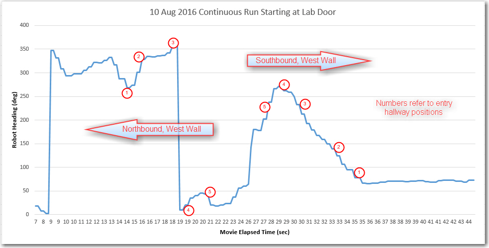
  • The data at each position corresponds well with data from the same position and orientation from the various continuous runs.  Given a continuous run and the knowledge of the interference pattern, it is possible to determine the robot’s location to a fair degree.  The following image shows the heading results from a 10 August continuous run, labelled with the position numbers from the entry hall layout diagram.  The positions were deduced from a movie of the run.
10 Aug continuous run, labelled with positions from the entry hall layout diagram

10 Aug continuous run, labelled with positions from the entry hall layout diagram

Conclusions:

  • The magnetometer and the heading calculation algorithm are probably working correctly
  • Magnetic interference is certainly a problem in the entry hallway next to the garage, and  may (or may not) be a problem elsewhere
  • Magnetic heading information may not be reliable/accurate enough to determine location with any precision, even coupled with left/right/front distances.

My next task is to run some continuous and step-by-step tests in other areas of the house, to determine if the entry hallway issue  is unique to the house or an ubiquitous problem.

Stay tuned!

Frank


OSU/STEM Outreach Speaker Amplifier Project, Part IV

Posted 04 August, 2016

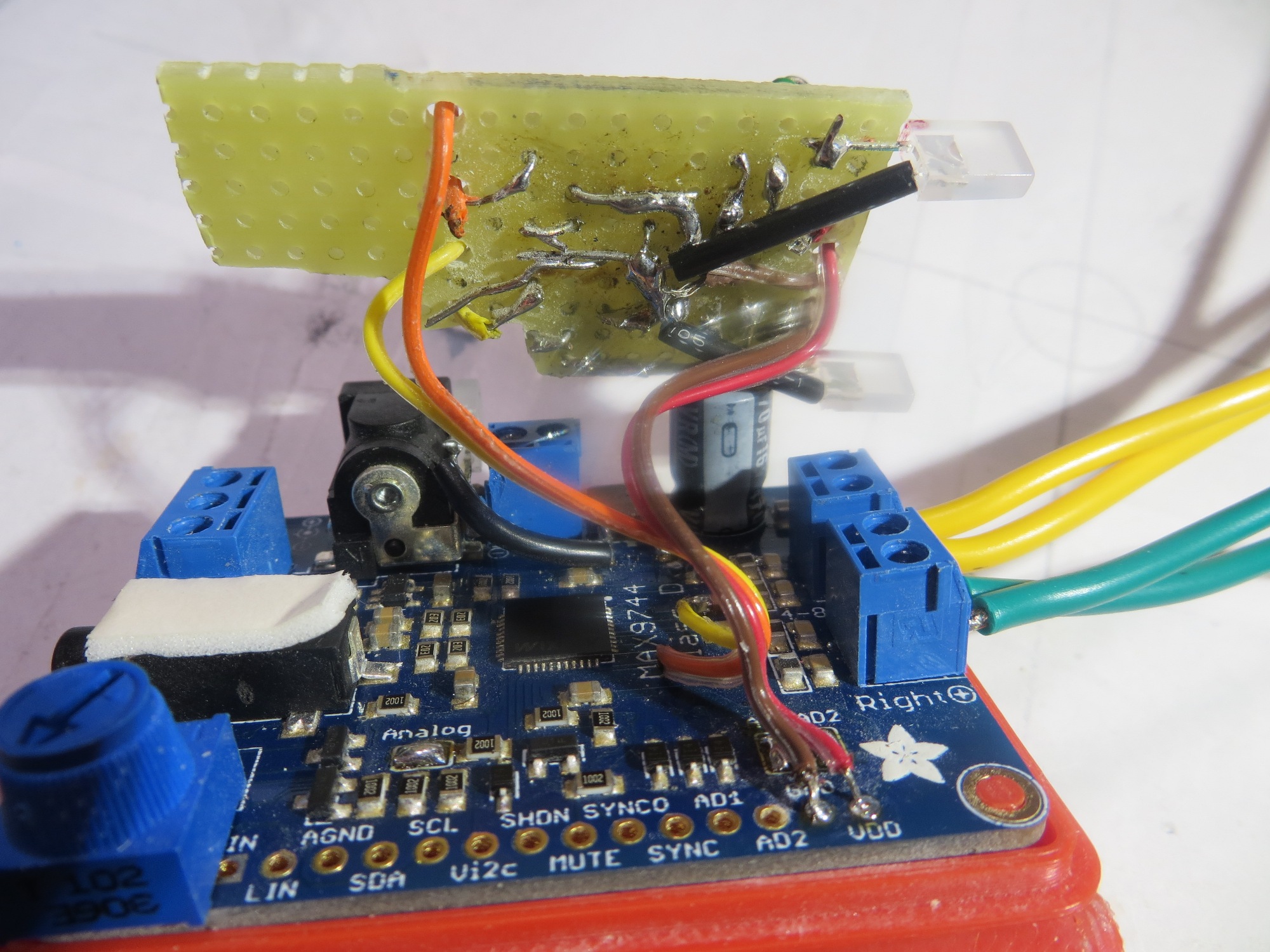
In my last post on this subject, I described the finishing touches on the project to design and fabricate a speaker amplifier for the OSU Engineering Outreach ‘paper speaker’ student project. The ‘finished’ project featured an audio activity monitoring circuit piggybacked onto the Adafruit 20W Class-D amplifier board, using my almost-forgotten  hand-wiring techniques on fiberglass ‘perf-board’, as shown in the following images.
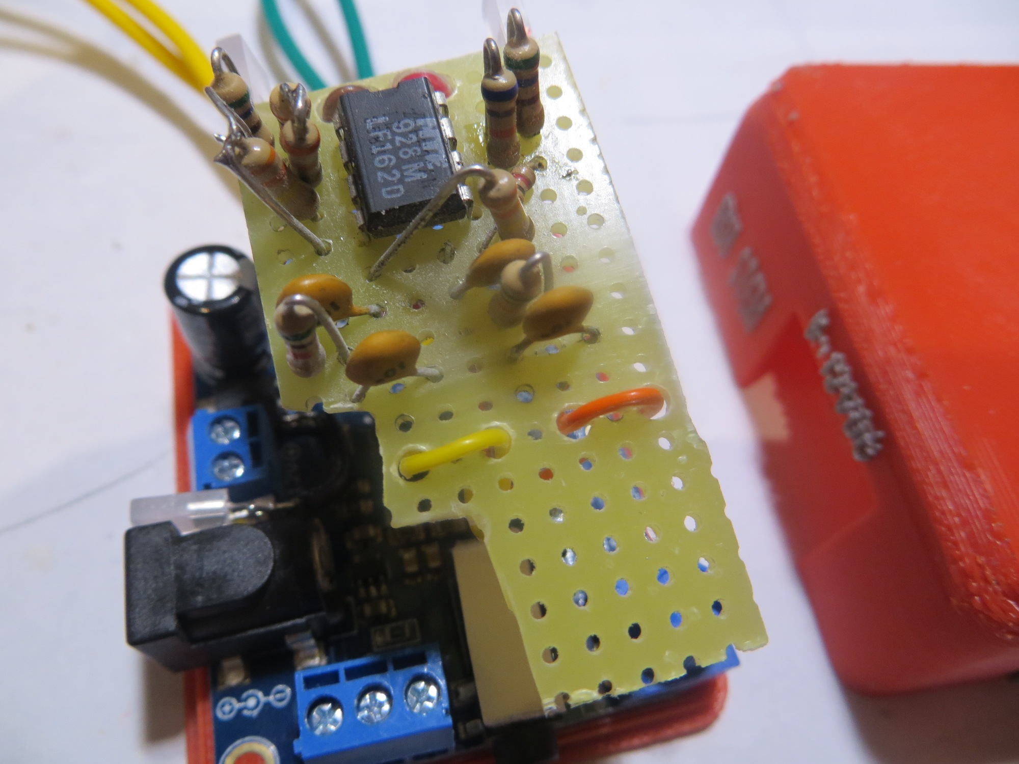
Cut-down perfboard, top view
Cut-down perfboard, top view

Cut-down perfboard, bottom view

Cut-down perfboard, bottom view

While this technique is perfect for a one-off project, I ultimately wanted to fabricate a number of these amplifier/monitor modules for use by the OSU Engineering Outreach team.  So, I decided to investigate the feasibility of obtaining a printed-circuit (PCB) board version of the LED monitor circuit, so I wouldn’t have to hand-fabricate the same circuit multiple times.  Of course, I knew in my heart that I could probably hand-fabricate ten (or a hundred) LED monitor circuits in the time it would take me to research the PCB design/fabrication field, acquire and learn a PCB design (aka EDA) package, actually design and implement the PCB, and then have the boards fabricated by a PCB house, but where’s the fun in that?

The last time I dealt with PCB design and manufacture was about 15 years ago while I was a researcher/JOAT (look it up) at The Ohio State University ElectroScience Laboratory, a research lab that specializes in Electromagnetics research and applications.  At the time I was a relatively new grad student at the lab (but one with about 30 years of electronics design  experience  in a prior lifetime with the CIA) and had somehow managed to get involved in a project that required some small-quantity PCBs.  The lab’s normal supplier (a local PCB manufacturing house) was still using hand-taping methods and the result was very high priced and of somewhat inconsistent quality (at least in my opinion), so I started looking for ‘a better way’.  In short order I found some low-cost, high quality EDA tools, and also found a small PCB house in Canada that would deliver small quantities in about 1/10 the time and 1/10 the cost as the local house. This made me a hero in the eyes of the lab director (but an enemy in the eyes of the guys who were comfortable dealing with the local supplier).  Anyway, it’s been another decade or so since I last looked at the EDA/PCB field,  so  I suspected things were even better now – and I wasn’t disappointed!

After a few hours of Googling, I found a number of posts that indicated that one of the better/easier-to-use EDA packages was Dip Trace, and they had a freeware version for those of us who can get by with 300 pins or less and only 2 signal layers – YAY!!  With a little further digging, I found some very complimentary reviews, so I downloaded the ‘free’ version and started trying to refresh  my PCB ‘game’.  Right away I found that DipTrace has a very complete and readable beginner’s tutorial, and unlike most ‘tutorials’ these days, the DipTrace one doesn’t skip steps – everything is explained and demonstrated in what had to seem like completely unnecessary detail to the experts, but in fact is absolutely crucial for a (almost) first-timer like me. If you are a hobbyist/enthusiast interested in PCB design/fabrication, I highly recommend DipTrace.

After working my way through most of the tutorial, I decided to try my hand at implementing my LED monitor circuit.  I started by porting my schematic from Digikey’s ‘scheme-it‘ (a free, browser-based schematic capture utility).  Here’s the schematic – first from Scheme-It, and then as it was ported to DipTrace.
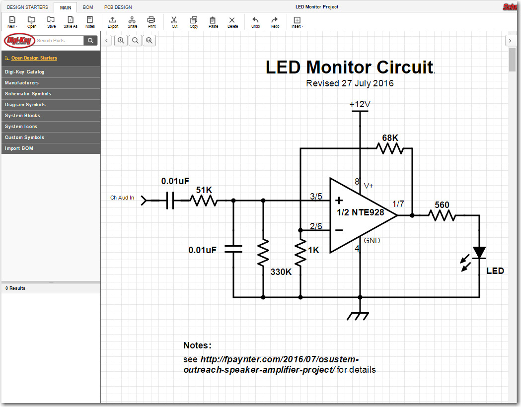
LED Monitor circuit schematic as captured in Digikey's 'Scheme-It' app

LED Monitor circuit schematic as captured in Digikey’s ‘Scheme-It’ app
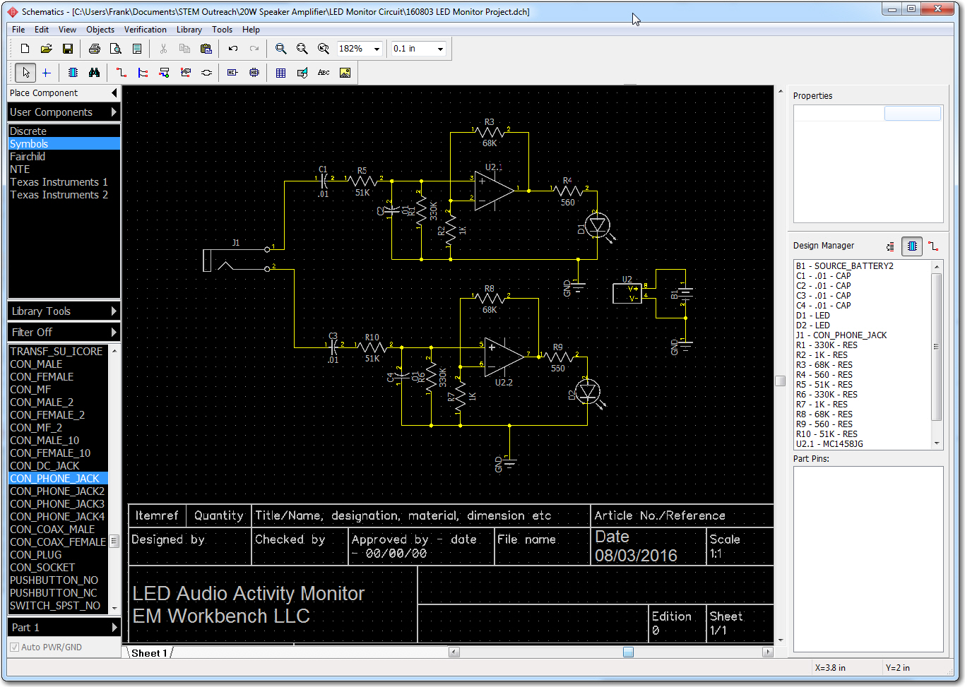
LED Monitor circuit schematic as captured in DipTrace

LED Monitor circuit schematic as captured in DipTrace

Following the procedure described (in exhaustive detail – YAY!) in the DipTrace tutorial, I then created an initial PCB design using ‘File -> Convert to PCB’ (or Ctrl-B) in the schematic capture app. This launches the PCB designer, and presents an initially disorganized parts layout as shown below.
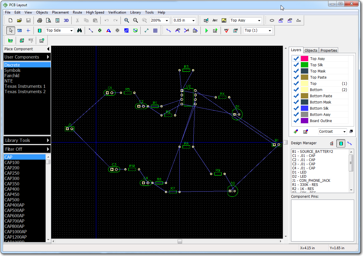
Initial PCB layout

Initial PCB layout

Had it not been for the great tutorial, this mishmash of parts would have been a real turnoff; fortunately, the tutorial had already covered this, so I knew to ‘keep calm and carry on’ by selecting ‘Placement -> Arrange Components’ from the main menu, which resulted in this much more compact and reasonable arrangement.
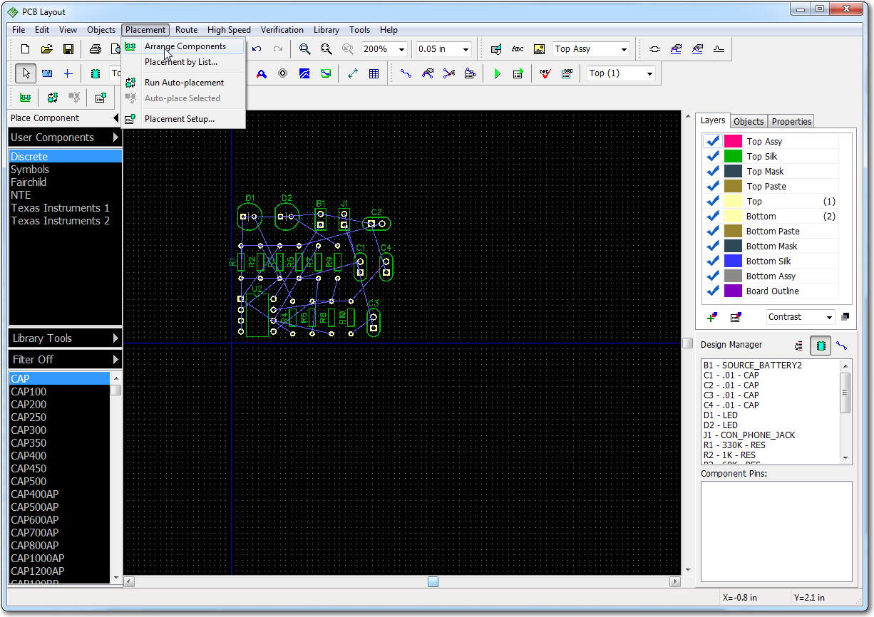
After 'Placement->Arrange Components'

After ‘Placement->Arrange Components’

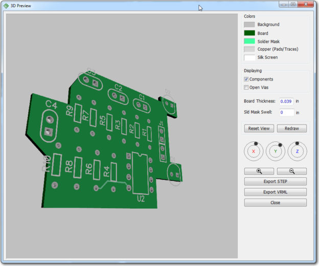
Working back and forth between the tutorial, the actual Adafruit 20W amplifier board, and the PCB design/layout screen, I was able to arrive at a final PCB design that implemented the entire circuit in a form factor that fit into the space available, as shown below.
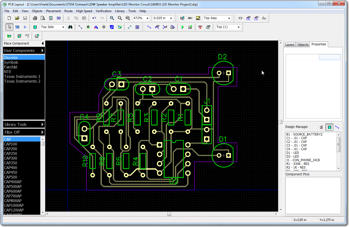
Finished PCB layout. Note the purple board border is customized to fit on top of the Adafruit amp board

Finished PCB layout. Note the purple board border is customized to fit on top of the Adafruit amp board

The above layout was significantly customized to fit on top of the Adafruit 20W amp board and in the 3D-printed enclosure.   This required a number of iterations, but the process was well supported by DipTrace; in particular, the ability to print the layout on my local laser printer in 1:1 scale helped immensely, as I was able to cut it out with scissors and actually lay it on top of the amp board to check the fit.

I was curious about how close I came to the ‘free’ version limitation of 300 pins, so I displayed the ‘File->Layout Properties’ dialog as shown below.  From this it was obvious that I still have plenty of room to play with for future projects, although I did use both the available signal layers. ;-).
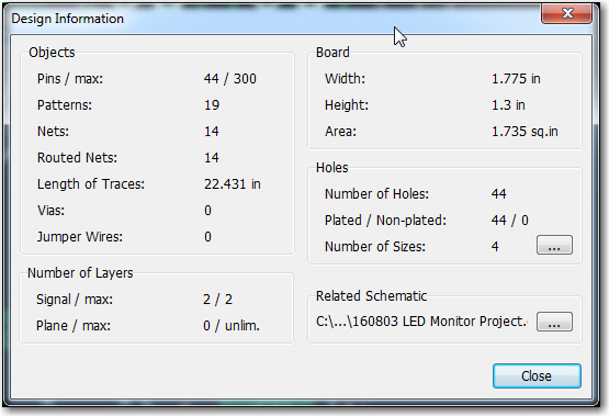
PCB properties, showing that this design fits well within the 300-pin maximum for the 'free' version

PCB properties, showing that this design fits well within the 300-pin maximum for the ‘free’ version

All in all, I probably spent 2-3 days from start to finish with DipTrace to get a finished PCB layout – not too shabby for an old broke-down engineer who can’t remember where he left his cane and hearing aids ;-).

But, all of this wasn’t even the really cool part of working with DipTrace!  The  really cool part came when I realized that DipTrace features a ‘baked-in’ link with Bay Area Circuits  for PCB procurement (File -> Order PCB…) as shown below
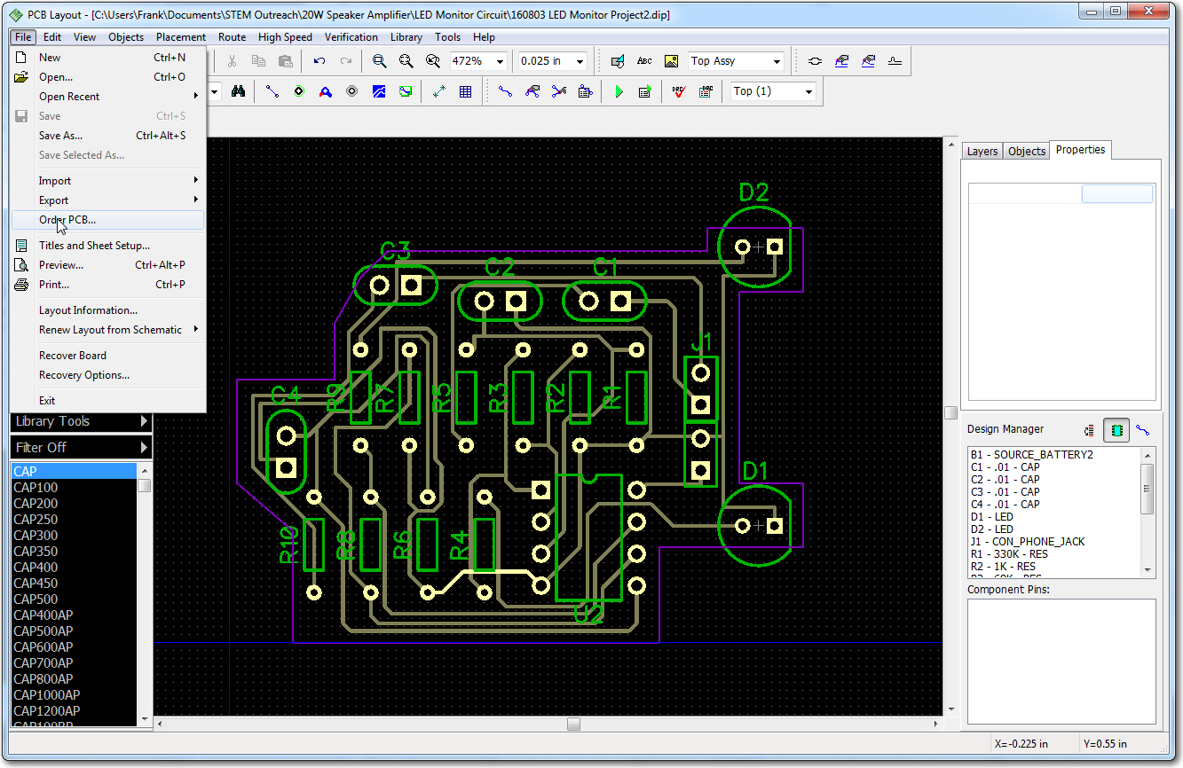
The 'File->Order PCB' menu item

The ‘File->Order PCB’ menu item

When you click on this option, the relevant data is scarfed up from the PCB layout information and you are presented with a simple ordering screen, complete with per-unit and total prices for your design.  All you have to do is select the quantity desired and press the ‘Place Order…’ button.  No messing with Gerber files, net lists, drilling schedules, mask layouts, etc etc.  One button, 30 bucks from my PayPal account – done!!!
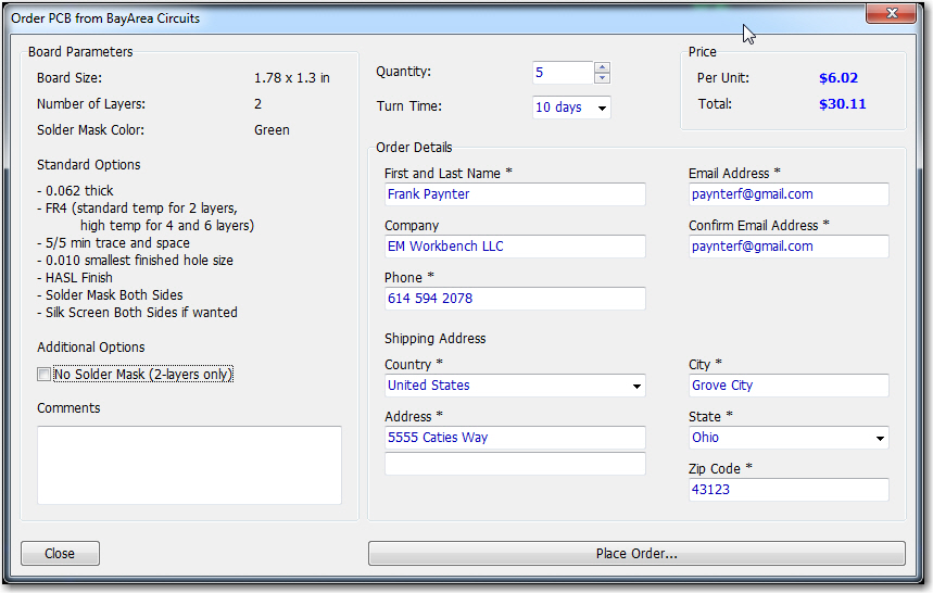
The order detail screen

The order detail screen

So, the lead time on the board order was quoted as about 10 days, so I won’t know for a couple of weeks how the whole thing worked out, but I’m quite optimistic.  I have to say that this was the most pleasurable and trouble-free PCB design project I have ever experienced, and I have experienced  a lot of them over the last 50 years, from hand-cut 10X mylar PCB masks, to hobbyist acid-baths, to $10,000 setup charge custom PCB shops, to this – wow!  I may never do another PCB project, but if I do, DipTrace will be my drug of choice!

Stay tuned,

Frank


Giving Wall-E2 A Sense of Direction, Part VIII

Posted 07/19/16

In my last post on this subject, I described moving my CK Devices ‘Mongoose’ IMU from a wooden stalk mounted on the 2nd deck to a more compact bracket mounted in the same location, and showed some data that indicated reasonable heading performance.  This post describes some ‘field’ (a hallway in my home) test results using the bracket-mounted configuration.

Field Test Site:

My ‘field test’ site consists of two hallway sections in my home. The two sections are oriented about 45 degrees to each other, as shown in the following diagram.

Field test area physical layout, oriented north-up

Field test area physical layout, oriented north-up

For my first ‘Field Test’, I simply set Wall-E2 loose at position 1, pointed in the direction shown in the diagram, and recorded via the  wixel-pair wireless connection implemented last December.  Wall-E2 successfully navigated (with a few ‘back-and-forth’ iterations) from point 1 to point 8 in the diagram, as shown in the following short video.

The captured telemetry data included the run time in seconds and the magnetic heading in degrees, and I sucked this information into Excel, where I graphed the mag heading versus time, as shown in the following screenshot.

Heading vs Time for Wall-E2 continuous run. Areas of puzzlement marked by '????'

Heading vs Time for Wall-E2 continuous run. Areas of puzzlement marked by ‘????’

As the caption notes, most of the graph makes sense, but there are at least two different areas where there is a more-or-less linear change of heading versus time, where there shouldn’t be any (or at least, where I don’t *think* there should be any).  Either Wall-E2 has some tricks up his sleeve that he wasn’t telling me about, or I don’t fully understand how the data and the physical record (the video) correspond.

OSU/STEM Outreach Speaker Amplifier Project, Part III


Posted 29 July 2016,

In my last post on this subject, I described the work to be completed to finish the OSU/STEM Outreach speaker amplifier project, as follows:

  • physically cut the perfboard down to a size that will fit into the enclosure, and figure out how it is to be secured.
  • Figure out how to mount the channel monitor LEDs so that they can be seen from outside the enclosure.  The plan at the moment is to mount them on the outside edge of the left and right screw terminals, respectively, and widen the AUD OUT opening enough so they can be easily viewed from outside.
  • Figure out how to route power and audio signals to the LED monitor board without using the external power and audio output screw terminals. The power wiring should be simple, as power and ground are available on the breakout pins provided by Adafruit.  However, the audio output signals are more problematic, as it isn’t obvious how to get to these circuit points, and I  really don’t want to start drilling holes in a multi-layer PCB.  After a careful visual inspection and some probing with my trusty DVM, I think I have located where I can safely tap into the PCB run from the last SMT resistor to the positive audio terminal for each channel – we’ll see!
  • Make sure the enclosure top fits OK, and all three LEDs are indeed visible.
  • Install semi-permanent L/R audio output cables with alligator clip terminations.  In actual use, I don’t really expect two paper speakers to be connected at once, but I’ll be ready if that situation occurs ;-).

Cut the perfboard down (and mount the LEDs):

With the help of my trusty Dremel tool and a carbide cutoff wheel, I trimmed the perfboard down to a size and shape that would fit into the enclosure, using the top surface of the audio input jack as a handy mating surface on one end, and with the monitor LEDs themselves as mounting legs on the other end, as shown in the following photos.

Cut-down perfboard, mounted front view

Cut-down perfboard, mounted front view

Cut-down perfboard, mounted, side view

Cut-down perfboard, mounted, side view

Power and audio signal wiring:

160729_LEDMonitorBoard1

Audio and power wiring

Audio and power wiring

Enclosure:

160729_LEDMonitorEncl4

Completed project shown connected to OSU paper speaker

Completed project shown connected to OSU paper speaker

Speaker connection cables:

Enclosure side view showing audio output connections

Enclosure side view showing audio output connections

All  Together Now…


So, at this point the amplifier project is all done  except for the ‘proof of the pudding’, which in this case is a real field test with real participants and student helpers.  If the field test results are satisfactory, I’ll probably build at least two more complete systems (I got 3ea amp boards from Adafruit and haven’t managed to kill any of them yet), and donate them to the OSU Engineering Outreach project.

Frank


OSU/STEM Outreach Speaker Amplifier Project, Part II

Posted 27 July 2016

In my last post on this subject, I had gotten to the point where I had a single-channel LED monitor circuit working, although it was still a bit  unkempt, to say the least.  In this post I describe the effort to get both channels working and to neaten everything up prior to installing the circuit into the speaker amplifier enclosure.

First off, I ‘improved’ the LED monitor circuit a bit, based on the results from testing the one-channel version.  I discovered there was a DC term riding on the class-D input signal, and this was getting amplified through the LED monitor circuit and swamping the audio  output at the LED.  So I added a 0.01uF DC blocking cap on the input line.  Unfortunately, this caused another problem, in that now the RC circuit cap had no discharge path so it almost immediately charged up and again swamped the audio signal.  One more addition – a 330K Ohm resistor across the low-pass cap to allow it to discharge.  Then, I adjusted the DC gain of the amp to provide a good  LED response to the audio.  I wanted the LED’s to come alive just about the time that a well-fabricated speaker produced clearly audible output.  The idea here is that a helper can tell immediately from the LEDs whether or not there is sufficient output power present to produce an audible response, and therefore if no response is detected, there is a problem with the speaker or the wiring from the amp to the speaker – but not upstream of that point.  After some fiddling around, I settled on a gain of about 70 for the LED monitor.  With that setup, and with the 20W amp gain set appropriately, I could easily drive the OSU paper speaker from my laptop, with the laptop’s audio output slider at about 50%.  The ‘New Improved’ LED monitor circuit is shown below:

Revised LED monitor schematic - one of two channels shown.

Revised LED monitor schematic – one of two channels shown.

The audio input to the monitor circuit is the rail-to-rail high-frequency (about 300KHz) audio-modulated PWM signal, as shown below

Amplifier output with audio input signal present

Amplifier output with audio input signal present

After the RC filter, only the audio signal is present, as shown in the following photo

LED monitor circuit audio input. Scope is set to 200mv/div

LED monitor circuit audio input. Scope is set to 200mv/div.

The following photo shows the output.  Due to the use of a single-supply op-amp and without any DC bias arrangement, only the positive input signal excursions produce an output – but that’s OK in this circuit as all we are doing is driving an LED.

LED monitor circuit LED drive signal. Only the positive audio transitions produce an output. Scope set to 2V/div

LED monitor circuit LED drive signal. Only the positive audio transitions produce an output. Scope set to 2V/div

While tweaking the monitor circuit, I had made quite a mess of my little perf-board layout.  So, after getting the schematic in good shape I basically tore everything down and started over again with the aim of building up the two-channel layout.  After everything was done, the result was the circuit shown in the following photo

Two-channel LED monitor circuit detail

Two-channel LED monitor circuit detail

two-channel LED monitor circuit in operation with the Adafruit 20W amp and the OSU paper speaker

two-channel LED monitor circuit in operation with the Adafruit 20W amp and the OSU paper speaker

After re-working the perf-board layout, adding the second channel, and carefully checking the wiring against the circuit, I was pleased to see that both channels operated as desired, and either channel could easily drive the OSU paper speaker.  The following short video shows the speaker being driven by the right channel, and both channel signals being monitored by the LED monitor circuit.


At this point the remaining work is:

  • physically cut the perfboard down to a size that will fit into the enclosure, and figure out how it is to be secured.
  • Figure out how to mount the channel monitor LEDs so that they can be seen from outside the enclosure.  The plan at the moment is to mount them on the outside edge of the left and right screw terminals, respectively, and widen the AUD OUT opening enough so they can be easily viewed from outside.
  • Figure out how to route power and audio signals to the LED monitor board without using the external power and audio output screw terminals. The power wiring should be simple, as power and ground are available on the breakout pins provided by Adafruit.  However, the audio output signals are more problematic, as it isn’t obvious how to get to these circuit points, and I  really don’t want to start drilling holes in a multi-layer PCB.  After a careful visual inspection and some probing with my trusty DVM, I think I have located where I can safely tap into the PCB run from the last SMT resistor to the positive audio terminal for each channel – we’ll see!
  • Make sure the enclosure top fits OK, and all three LEDs are indeed visible.
  • Install semi-permanent L/R audio output cables with alligator clip terminations.  In actual use, I don’t really expect two paper speakers to be connected at once, but I’ll be ready if that situation occurs ;-).

Once I’m sure everything is working OK and that the whole thing won’t die on me the first time someone looks at it sideways, then the plan is to volunteer for an upcoming speaker fabrication session and try the amp in the ‘real world’.  If it works as I fully expect it to, then the idea is to donate two or three to the OSU Engineering Outreach program, in the name of my company (EM Workbench LLC).  Stay tuned!

Frank
 

OSU/STEM Outreach Speaker Amplifier Project, Part I

Posted  July 25, 2016

Lately I have become involved in the Engineering Outreach program here at The Ohio State University, as a volunteer helper at ‘hands-on’ engineering project presentations to grade-school and middle-school students in the Columbus, Ohio area.  A week or so ago I helped out in a session where the students (middle-schoolers at a science day-camp) got to fabricate and test an audio speaker from a paper template, some magnet wire, and a couple of small permanent magnets, and I was struck by the difficulty the kids were having in actually hearing anything coming out of their freshly-fabricated speakers when they connected them to the output of their phones and/or iPads.  I could understand if I couldn’t hear anything – I’m an old power pilot and my ears are shot from thousands of hours of piston engine noise – but the kids with their brand-new ears couldn’t hear anything either!  There was an audio amplifier available for the kids to use, but it wasn’t much help either – there wasn’t any indication that the amp was actually doing anything, so it could have died long ago and nobody would ever know – bummer.  Anyway, I came away from that project with the distinct impression that this particular project wasn’t doing much for the kids, and maybe I could do something to help.  So, before I left the room, I made a point of ‘borrowing’ all the parts required to fabricate my own paper speaker – the paper template, magnet wire, and permanent magnets along with the other small bits and pieces.

My first line of inquiry in my own home lab was to determine what the best fabrication technique was for the speaker itself.  My thinking was that since this project has been around forever in one guise or another, it sorta  had to be successful in some sense, or it would have died out long ago.  Therefore, I reasoned that a more careful approach to the actual fabrication might yield better results.  After doing some inet research, I realized that one of the critical aspects of paper speaker construction is to make sure the speaker coil assembly (a section of plastic straw hot-glued to the speaker cone with the magnet wire wound around it’s lower end) was free to move vertically – i.e. it wasn’t forced down against the baseplate by the tension of the speaker legs.  In other words, the speaker legs had to be arranged such that the speaker coil assembly floated 2-3  mm above the base.  After playing with this a while, I realized that the proper technique was to arrange the speaker legs so as to properly suspend the coil assembly first, and then place the permanent magnet ‘dot’ under the coil assembly second, rather than the other way around.  Assembly in this sequence tends to minimize lateral friction of the coil assembly straw section against the side of the permanent magnets, hopefully resulting in higher mechanical/audio transfer efficiency.

After constructing the speaker as carefully as possible, I hooked it up to my laptop audio output, and voila! – no audio :-(.  Even with the audio output at max volume (which, when directed to my laptop’s internal speakers is enough to vibrate my workbench), it was almost impossible to hear anything from the speaker.  Even with careful construction with no time constraints, and a top-end audio source, getting the speaker to work was a very marginal deal.

After thinking about this for a while, I decided that I was maybe working the wrong end of the system.  What I needed to do was to implement an audio amplifier that would provide sufficient output power so that even a marginally constructed speaker would work properly; the only real limitation on power that I could see would be the current limit imposed by the magnet wire itself – as long as I didn’t physically melt the wire, I should be OK! ;-).

My first try at an amplifier was based around a power MOSFET I had lying around, as shown in the following photo.  1607_MOSFET_AMP

This worked ,but only up until the point at which the drain resistor started smoking!  That’s the problem with a linear amplifier driving a speaker – LOTS of power being dissipated.

So, back to the drawing board, with more inet research.  This time, I came across the  very nice Adafruit  Class-D speaker amplifier  shown below.  The kit has everything needed to build a complete speaker amp, as shown in the second image below.  The amplifier runs Class-D, so it is very efficient, and it depends on the speaker coil inductance to  reject the high-frequency switching signal, leaving only the audio.


Adafruit 20W Class-D speaker amplifier, based on the MAX9744 amplifier chip

Adafruit 20W Class-D speaker amplifier, based on the MAX9744 amplifier chip

Adafruit 20W Class-D speaker amplifier application

Adafruit 20W Class-D speaker amplifier application

The folks at Adafruit were even thoughtful enough to provide the STL file for a 3D-printable enclosure for the amp, as shown below:

3D-printable enclosure for the 20W Class-D amp

3D-printable enclosure for the 20W Class-D amp

And, since I am the proud owner of not just one, but  two 3D printers (a Printrbot Simple Metal, and a PowerSpec 3D Pro/aka Flashforge Creator X), the existence  of a ready-made design for the enclosure saved some time.

After receiving my amps from Adafruit, and after the requisite amount of fumbling around, I managed to get the amp running and connected to a couple of old speakers.  When I connected up my laptop’s audio output I was quite pleased that, even at the default 6dB gain setting, the amp easily drove the speakers to the point where I had to reduce the audio input volume to avoid complaints from the wife in the next room.

Adafruit amp test setup

Adafruit amp test setup

At this point, it was clear that the Adafruit amp should be an excellent solution to the paper-speaker driver problem, but I wasn’t quite done yet.  There were still several  remaining issues:

  • The amplifier used in the previous sessions had no ‘power ON’ indication, so there was no way to tell if the thing was actually operating or not.  The Adafruit amp, as delivered doesn’t have one either, so this had to be corrected somehow.
  • The previous amplifier had no ‘audio activity’ indication, so even if you somehow knew that it was indeed getting  power and working, there wasn’t any way to tell if there was any audio output without  attaching a speaker; and if there was no sound, there was no way to tell if the problem was the speaker or the amp.
  • The original enclosure design by Adafruit didn’t actually fit – the slots for the power and audio-in jacks weren’t high enough (later design change?). In addition, there were no provisions for either the ‘power ON’ or ‘audio activity’ indicators.  Fortunately I not only have 3D printers, but an account on TinkerCad  so the design could be adjusted.
  • Since I still haven’t actually connected the amp to my paper speaker, I don’t really know yet if the default 6dB gain setting is sufficient to drive the speaker; I may still have to change to the analog gain setup and use a higher gain setting (fortunately, Adafruit thoughtfully provided a 1K potentiometer and a set of jumper pads to achieve this, if necessary).

Power-ON Indication:

The power-ON indication issue was fairly easy to address – all I had to do was add an LED-resistor combination across the external power input lines.   The only problem with this solution was finding a way for the LED to be visible outside the enclosure – and the solution was to modify the enclosure design to expose the external power screw terminals (they were hidden in the original design), and in the process leave a bit of space open between the power input jack  and the screw terminal, a space just wide enough for a small, rectangular LED as shown below.

Power ON indicator LED installed between power input jack and external power screw terminals

Power ON indicator LED installed between power input jack and external power screw terminals

Audio Activity Indicator:

The Adafruit amplifier is Class-D – i.e.  the output is a pulse-width-modulated (PWM) signal, as shown below:

Amplifier output with audio input signal present

Amplifier output with audio input signal present

Amplifier output with no audio input signal present

Amplifier output with no audio input signal present

As can (or more accurately,  cannot) be seen from the above photos, there is no appreciable difference between the ‘audio’ and ‘no audio’ waveforms.  The class D amplifier technique depends on the low-pass nature of the speaker coil to suppress  the high-frequency switched waveform  terms, leaving only the audio term.  Unfortunately, this means there really isn’t anything there to directly drive an audio activity indicator – the typical LED is plenty fast enough to follow the high-frequency PWM waveform, thereby masking the audio signal.  One possible technique would be to sample the speaker coil current (which pretty much by definition doesn’t contain the high-frequency switching terms), but this requires that a working speaker be attached.  This won’t work, because the whole idea of an audio activity indicator is to confirm that an audio input is present and has been amplified sufficiently to adequately drive a speaker  before one is connected.  So, I decided to try a simple RC low-pass filter, followed by a basic audio amplifier to drive the activity LED.  The circuit for one channel is shown below.

LED monitor circuit for one channel

LED monitor circuit for one channel.  Pin numbers are Channel1/Channel2

Here is a short video showing the LED monitor circuit in action


So, at this point I have a working speaker amplifier, a power-ON indicator, and at least the prototype of an audio activity monitoring circuit.  Next up – finish the LED monitor circuit, finish the enclosure design and fabrication, and assemble everything for delivery.